One of the most common application problems is the absence of a direct current (DC) loop that provides a bias current in an alternating current (AC) coupled operational amplifier or instrumentation amplifier circuit. In Figure 1, a capacitor is placed in series with the non-inverting input of the op amp for AC coupling, a simple way to isolate the DC component of the input voltage (VIN). This is especially useful in high gain applications where even small DC voltages at the op amp input limit the dynamic range and even cause output saturation. However, adding a capacitive coupling to the high-impedance input without providing a DC path for the current at the non-inverting input can cause problems.
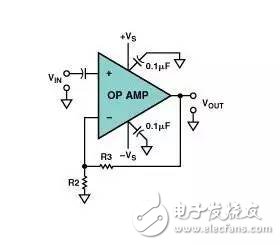
Figure 1. Wrong op amp AC coupling
In effect, the input bias current flows into the coupled capacitor and charges it until it exceeds the nominal value of the common-mode voltage of the amplifier input circuit or limits the output. Depending on the polarity of the input bias current, the capacitor will charge to the positive or negative voltage of the power supply. The closed loop DC gain of the amplifier amplifies the bias voltage.
This process can take a long time. For example, a field effect transistor (FET) input amplifier with a charge current I/C of 10–12/10–7=10 μV/s when a bias current of 1 pA is coupled to a 0.1μF capacitor, or 600 μV minutes. If the gain is 100, the output drift is 0.06 V per minute. Therefore, general laboratory testing (using an AC-coupled oscilloscope) does not detect this problem, and the circuit does not experience problems until after a few hours. Obviously, it is very important to avoid this problem altogether.
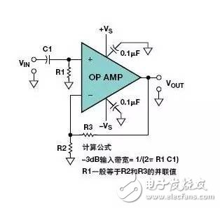
Figure 2. The correct dual-supply operational amplifier
AC coupled input method
Figure 2 shows a simple solution to this common problem. Here, a resistor is connected between the input of the op amp and ground to provide a ground loop for the input bias current. In order to minimize the offset voltage caused by the input bias current, when using a bipolar op amp, the bias current of the two inputs should be equal, so the resistance of R1 should normally be set equal to the parallel resistance of R2 and R3. value.
However, it should be noted that this resistor R1 always introduces some noise into the circuit, so a trade-off is made between the circuit input impedance, the size of the input coupling capacitor, and the Johnson noise caused by the resistor. Typical resistor values ​​are typically between 100,000 Ω and 1 MΩ.
Similar problems can occur in the instrumentation amplifier circuit. Figure 3 shows an instrumentation amplifier circuit that uses two capacitors for AC coupling without providing a return path for the input bias current. This problem is common in instrumentation amplifier circuits powered by dual power supplies (Figure 3a) and single power supplies (Figure 3b).
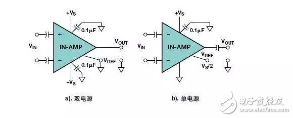
Figure 3. Example of an inactive AC-coupled instrumentation amplifier
This type of problem can also occur in transformer-coupled amplifier circuits, as shown in Figure 4. This problem can occur if a DC-to-ground loop is not provided in the transformer secondary circuit.
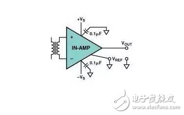
Figure 4. Transformer-coupled instrumentation amplifier circuit that is not working
Figures 5 and 6 show a simple solution for these circuits. Here, a high-resistance resistor (RA, BR) is connected between each input and ground. This is a simple and practical solution for dual power instrumentation amplifier circuits.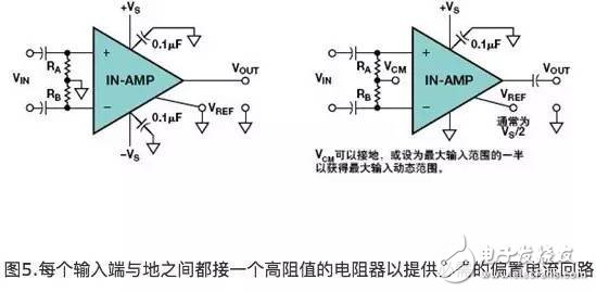
a. Dual power supply. b. Single power supply.
These two resistors provide a discharge loop for the input bias current. In the dual power supply example shown in Figure 5, the reference terminals of both inputs are grounded. In the single-supply example shown in Figure 5b, the reference terminals of the two inputs are either grounded (VCM grounded) or connected to a bias voltage, typically half the maximum input voltage.
The same principle can be applied to a transformer-coupled input circuit (see Figure 6), unless the secondary of the transformer has a center tap that can be grounded or connected to VCM.
In this circuit, a small offset voltage error occurs due to a mismatch between the two input resistors and/or a mismatch in the input bias current across the two terminals. In order to minimize the offset error, a resistor can be connected between the two inputs of the instrumentation amplifier (that is, bridged between the two resistors), and its resistance is about 1/10 of the first two resistors ( However, it is still large compared to the differential source impedance).
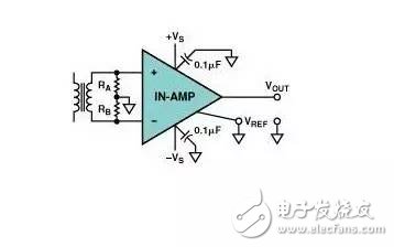
Figure 6. Correct Instrumentation Amplifier Transformer Input Coupling Method
Provides reference voltages for instrumentation amplifiers, operational amplifiers, and ADCs
Figure 7 shows a single-supply circuit in which an instrumentation amplifier drives an analog-to-digital converter (ADC) with a single-ended input. The amplifier's reference voltage provides a bias voltage for a zero differential input, while the ADC's reference voltage provides a scaling factor. A simple RC low-pass anti-aliasing filter is typically placed between the output of the instrumentation amplifier and the input of the ADC to reduce out-of-band noise. Design engineers often want to use simple methods such as resistor dividers to provide reference voltages for instrumentation amplifiers and ADCs. Therefore, when using some instrumentation amplifiers, errors will occur.
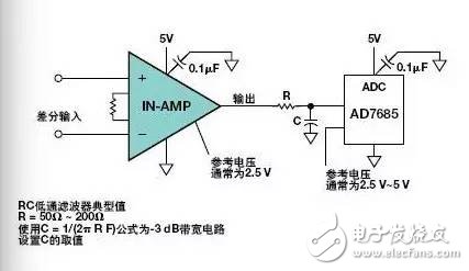
Figure 7. Typical single-supply circuit for an ADC driven by an instrumentation amplifier
Properly provide the reference voltage of the instrumentation amplifier
It is generally assumed that the reference input of the instrumentation amplifier is high impedance because it is an input. Therefore, design engineers generally want to connect a high-impedance source, such as a resistor divider, to the reference pin of the instrumentation amplifier. This can cause serious errors in the use of certain types of instrumentation amplifiers (see Figure 8).
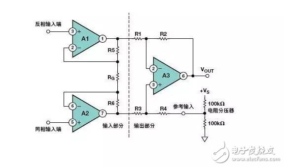
Figure 8. Incorrectly using a simple resistor divider to directly drive the reference voltage of the 3 op amp instrumentation amplifier
For example, the popular instrumentation amplifier design configuration uses the three op amp structure shown above. The total signal gain is

The gain at the reference voltage input is 1 (if input from a low impedance voltage source). However, in the circuit shown above, the reference input pin of the instrumentation amplifier is directly connected to a simple voltage divider. This will change the symmetry of the subtractor circuit and the voltage divider ratio of the voltage divider. This also reduces the common-mode rejection ratio of the instrumentation amplifier and its gain accuracy. However, if R4 is connected, the equivalent resistance of the resistor will become smaller, and the reduced resistance value is equal to the resistance value (50 kΩ) seen from the two parallel branches of the voltage divider. The circuit behaves as one size. A low-impedance voltage source that is half the supply voltage is applied to the original value R4, and the accuracy of the subtractor circuit remains unchanged.
This method cannot be used if the instrumentation amplifier is in a closed single package (one IC). Also, consider that the temperature coefficient of the divider resistor should be the same as the resistor in R4 and the subtractor. Finally, the reference voltage will not be adjustable. On the other hand, if you try to reduce the resistance of the voltage divider resistor, the increased resistance is negligible, which increases the power supply current consumption and the power consumption of the circuit. In any case, this clumsy method is not a good design.
Figure 9 shows a better solution by adding a low-power op amp buffer between the voltage divider and the instrumentation amplifier's reference voltage input. This eliminates the problem of impedance matching and temperature coefficient matching, and it is easy to adjust the reference voltage.
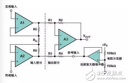
Figure 9. Using the low output impedance op amp to drive the reference voltage input of the instrumentation amplifier
PSR performance should be guaranteed when using a voltage divider to supply a reference voltage to the amplifier from the supply voltage
A frequently overlooked problem is that any noise, transients or drift of the supply voltage VS will be applied directly to the output via the reference input as a function of the voltage division ratio. Practical solutions include bypass filtering and even reference voltages generated using precision reference voltage ICs, such as the ADR121, instead of VS divider.
This consideration is important when designing circuits with instrumentation amplifiers and operational amplifiers. Supply voltage suppression techniques are used to isolate the amplifier from hum, noise, and any transient voltage variations in its supply voltage. This is very important because many of the actual circuits are included, connected, or exist in an environment that only provides a non-ideal supply voltage. In addition, the AC signal in the power line is fed back into the circuit to be amplified, and under appropriate conditions can cause parasitic oscillations.
Modern op amps and instrumentation amplifiers offer relatively low frequency supply voltage rejection (PSR) capabilities as part of their design. This is taken for granted by most engineers. Many modern op amps and instrumentation amplifiers have PSR specifications above 80 to 100 dB, which can attenuate the effects of supply voltage variations to 1/10,000 to 1/100,000. Even the most appropriate 40 dB PSR amplifier isolation can have a 1/100 rejection of the power supply. However, high frequency bypass capacitors (as shown in Figures 1-7) are always required and often play an important role.
In addition, when a design engineer uses a simple supply voltage resistor divider and uses an op amp buffer to provide a reference voltage for the instrumentation amplifier, any change in the supply voltage is passed directly through the circuit to the output stage of the instrumentation amplifier without attenuation. . Therefore, unless a low pass filter is provided, the IC typically has excellent PSR performance loss.
In Figure 10, a large capacitor is added to the output of the voltage divider to filter out variations in the supply voltage and to ensure PSR performance. The -3 dB pole of the filter is determined by the parallel connection of resistor R1/R2 and capacitor C1. The -3 dB pole should be set at 1/10 of the lowest useful frequency.
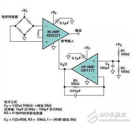
Figure 10. Reference End Decoupling Circuit to Ensure PSR Performance
The CF trial value shown above is capable of providing a –3 dB pole frequency of approximately 0.03 Hz. A small capacitor (0.01 μF) connected across R3 minimizes resistor noise.
This filter takes time to charge. According to the trial value, the rise time of the reference input should be several times the time constant (here T=R3Cf= 5 s), or 10~15s.
The circuit in Figure 11 has been further improved. Here, the op amp buffer acts as an active filter that allows the use of capacitors with much smaller capacitance values ​​to decouple the same large supply. In addition, an active filter can be used to increase the Q value to speed up the on-time.
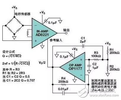
Figure 11. Connecting the op amp buffer to the active filter to drive the reference input pin of the instrumentation amplifier
Test Results: Using the component values ​​shown above, apply a 12 V supply voltage to filter the 6 V reference of the instrumentation amplifier. Set the gain of the instrumentation amplifier to 1 and modulate the 12 V supply with a frequency-changing 1 VP-P sinusoidal signal. Under such conditions, as the frequency decreases, it is reduced to approximately 8 Hz, and we do not see the AC signal on the oscilloscope. When applying a low amplitude input signal to an instrumentation amplifier, the circuit's test supply voltage range is 4 V to 25 V or higher. The on-time of the circuit is approximately 2 s.
Decoupling of single-supply operational amplifier circuits
Finally, a single-supply op amp circuit needs to bias the common-mode input voltage amplitude to control the positive swing and negative swing of the AC signal. When the bias voltage is supplied from the supply voltage using a voltage divider, proper decoupling is required to ensure the performance of the PSR.
A common but incorrect method is to provide a VS/2 to the non-inverting input of the op amp using a 100 kΩ/100 kΩ resistor divider (plus a 0.1μF bypass capacitor). Decoupling the supply with such a small capacitance value is usually not enough because the pole is only 32 Hz. The circuit is unstable ("low frequency oscillation"), especially when driving inductive loads.
Figure 12 (inverting input) and Figure 13 (in-phase input) show the VS/2 bias circuit that achieves the best decoupling results. In both cases, the bias voltage is applied to the non-inverting input, fed back to the inverting input to ensure the same bias voltage, and the unit DC gain is also biased by the same output voltage. Coupling capacitor C1 reduces the low frequency gain from BW3 to unity gain.
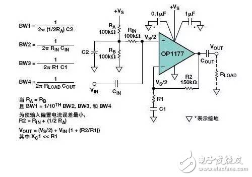
Figure 12. The correct power supply decoupling scheme for a single-supply, non-inverting input amplifier circuit. IF gain = 1 + R2 / R1
As shown in the figure above, a good rule of thumb when using a 100 kΩ/100 kΩ resistor divider is that the minimum C2 should be 10 ΩF to achieve a –3 dB cutoff frequency of 0.3 Hz. And 100 μF (0.03 Hz) is actually sufficient for all circuits.
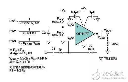
Figure 13. Correct decoupling circuit for a single-supply inverting input amplifier with IF gain = – R2/R1
The utility model relates to a medical atomization treatment and humidifying device belonging to the technical field of medical equipment and household appliances.
Professional Medical Atomization manufacturer is located in China, including Medical Vape,Dose Control Vape Pen,Supersonic Wave Vape, etc.
Medical Atomization,Medical Vape,Dose Control Vape Pen,Supersonic Wave Vape
Shenzhen MASON VAP Technology Co., Ltd. , https://www.cbdvapefactory.com