Abstract: When the output of the hot-swap control circuit is short-circuited, the internal circuit breaker function is triggered and the circuit is opened. But before the internal circuit breaker reacts, the short-circuit current at the beginning may reach hundreds of amperes. Usually the delay time of the hot-swap controller circuit breaker is 200ns to 400ns, coupled with the limited gate pull-down current, the gate turn-off time may require 10µs to 50µs. During this period, a large short-circuit current will occur.
This application note presents a simple external circuit that minimizes the initial current spike and isolates short-circuit faults within 200 to 500ns.
Typical hot-swap circuit Let's examine the + 12V, 6A typical hot-swap control circuit built with MAX4272 (Figure 1). According to the specifications of the MAX4272, it can be seen that it includes low-speed and fast comparators with trigger thresholds of 50mV and 200mV respectively (over the entire temperature range, tolerances are 43.5mV to 56mV and 180mV to 220mV, respectively). The trigger current is usually 1.5 to 2.0 times the operating current, select RSENSE = 5mΩ. RSENSE allows a tolerance of 5%. The trigger current range of the low-speed comparator under overload conditions is 8.28 to 11.76A; when a short circuit occurs, the trigger current range of the fast comparator is 34A to 46.2A.
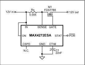
Figure 1. Typical hot-swap control circuit
The minimum trigger threshold of the low-speed comparator is 38% higher than the normal operating current, and the short-circuit trigger threshold of the fast comparator is 6 to 8 times the operating current.
The delay time of the fast comparator is 350ns, and the short-circuit current spike during this period is limited only by the circuit impedance. After that, the current slowly decreases until the short-circuit fault is completely isolated. The 3mA gate pull-down current limits the discharge rate of the MOSFET M1 gate capacitance (3nF to 4nF). The short-circuit current slowly decreases from 15µs to 40µs, and at the same time, the gate voltage is pulled from 19V to near ground potential. Peak short-circuit current The initial peak current within 350ns is determined by the following factors:
(a) Power supply ESR, (b) Short-circuit state, (c) RSENSE resistance, (d) M1 RDS (ON), (e) M1 ID (ON).
The above parameters adopt the values ​​closest to the actual situation, and the total impedance of the circuit during short circuit can be calculated:
(Power supply ESR ≈ 4mΩ) + (Short circuit ≈ 3mΩ) + (RSENSE = 5mΩ) + (RD (ON) ≈ 4mΩ) ≈ 16mΩ.
At this time, the short-term peak current is: ISC ≈ 750A, and depends on the energy storage capacitor of the power supply (when the low ESR backplane with a 2200µF capacitor is discharged at 750A, the voltage within 1µs will only decrease by 340mV). In this case, the actual peak ISC will be limited to about 400A by M1's ID (ON).
ID (ON) depends on VGS, so it is necessary to check the circuit to determine the gate-source voltage during this period. The MAX4272 includes an internal charge pump that allows the gate voltage during normal operation to be about 7V higher than VIN. Therefore, when the MOS tube is turned on, VGS = 7V.
The second effect of the short circuit is that it actually increases VGS. The short circuit introduces a voltage step between the drain and source of M1-equal to a part of the total input voltage. Since the RD (ON) of M1 is about 1/3 of the estimated total impedance of the short circuit, the VDS applied at this time is about 1/3 of the 12V step voltage. The voltage divider composed of the drain-gate capacitance cdg and the gate-source capacitance cgs will transfer a part of this step voltage to the gate. After proper calculations, it can be seen that the additional ΔVGS introduced is 300mV to 500mV, but tests conducted during the short circuit show that this value can be as high as ΔVGS = + 3V.
At this point, it can be clearly seen that a solid and reliable short circuit can generate hundreds of amperes of current in a few microseconds to tens of microseconds.
Designers may wish to limit the peak ISC to 50A for a duration of less than 1µs, but this requirement is impractical without adding faster comparators and gate pull-down circuits. However, some simple modifications to the circuit can be considered. During the initial 350ns response time of the internal fast comparator, the current will be limited to a few hundred amperes by ID (ON). In this case, a simple external circuit can be added to speed up the gate discharge, thereby limiting the short circuit duration to ≤ ½µs . Or use a slightly more complicated external circuit to limit the peak Isc to 100A, and the duration is ≤ 200ns. The fast gate pull-down circuit limits the duration of the large short-circuit current by simply adding a PNP Darlington tube Q1, which can greatly shorten the duration of the large short-circuit current, as shown in Figure 2. Diode D1 allows the gate to charge normally in the on state, while the controller discharges the 3mA gate discharge current to directly drive the base of Q1 when it is off. Then Q1 quickly completes the gate discharge in about 100ns. In this way, the duration of the large current when the short circuit occurs is greatly shortened, which is only slightly longer than the 350ns delay time of the fast comparator.
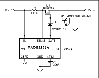
Figure 2. Hot-swap controller with fast gate pull-down. Fast current limiting circuit With the circuit shown in Figure 3, the short-circuit current can be limited to less than about 100A for a duration of less than 200ns. When the voltage difference across RSENSE reaches about 600mV, the PNP transistor Q1a will trigger and drive the NPN transistor Q1b, thereby quickly discharging the gate capacitance of M1.
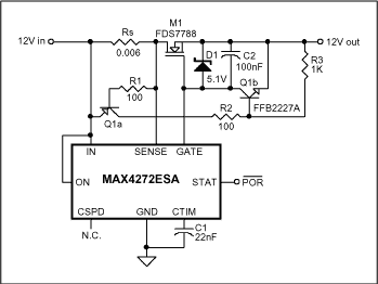
Figure 3. Hot-swap controller with fast short-circuit peak current limit
C2 between the gate and source of M1 can further reduce the forward transient step voltage applied to the gate when a short circuit occurs. The value of this capacitor ranges from 10nF to 100nF.
Zener diode D1 is used to limit VGS to a value below 7V (MAX4272 provides this voltage).
Although the Zener diode D1 is rated at 5.1V at a bias current of 5mA, in this circuit, the MAX4272 can only output a gate charge current of 100µA (Zener diode bias current), so D1 limits VGS At about 3.4V. Restricted VGS can reduce ID (ON), and of course RD (ON) will increase. According to the data of MOS tube: RD (ON) is 5mΩ when VGS is 3.4V, and RD (ON) is 3mΩ when VGS is 7V. This can turn off M1 faster.
D1 and C2 can also be used in the circuits of Figure 1 and Figure 2 to reduce the ID (ON) during short circuit. Test Method-There is nothing easier to create a short circuit than to make a short circuit.
However, it is very challenging to produce a reliable, reliable, and repeatable short circuit. This test evaluates the following methods of making short circuits. When the mechanical switch is closed, there will always be a few milliseconds of contact vibration process. Rotary multi-contact switches seem to avoid similar situations, but because the electric sparks formed by multiple large current closures will corrode the contacts, the repeatability of the switch is doubtful. High-current relay contacts also produce jitter when closed, and will exhibit different closing resistances. The experiment proves that the current rising rate of the thyristor is not satisfactory. High-current mercury displacement relays are the best method people have high hopes, but the results are not satisfactory. A 60A, 600V mercury relay with a nominal impedance of 4mΩ has an impedance of 40mΩ at the beginning of contact, and will easily drop to 4mΩ as the current pulse flows for 15µs. Manual short-circuit operation can provide a random, intermittent and non-repetitive shorting method, with strong randomness! A very steep current wave front can be obtained. In summary, although contact corrosion has an impact on the repeatability of each closure, this method is still the most effective (and most economical). The most feasible laboratory method is to use multiple large output CMOS Schmitt line drivers to drive multiple parallel, low RD (ON), NMOS transistors. Due to time and resource constraints, this option was not adopted.
It is extremely difficult to consistently produce true low-resistance short-circuit faults with steep current fronts by mechanical means in the laboratory. The circuit will almost certainly experience this unexpected short-circuit fault when it is in operation.
Usually artificial short circuit will produce the capacitor discharge current and voltage waveform as shown in Figure 4. The upper curve is the short-circuit output voltage recorded when 5V / div is selected. It can be seen that most of the time (25µs / div) the capacitor discharges less than half. The lower curve is the short-circuit current recorded when the 25A / div gear is selected, which clearly shows that the contact is intermittent.
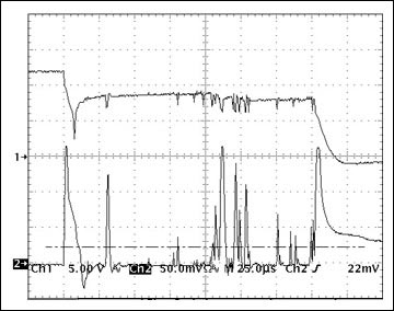
Figure 4. Irregular mechanical short circuit signal waveform
It is not easy to construct a power supply with an ESR lower than 5mΩ. Despite this, every effort has been made to construct a low ESR (4-5mΩ) voltage source. After careful measurement, it can be seen that the voltage drops by 440mV in the case of a 100A short circuit. The input of the voltage source is directly connected in parallel with a 5500µF computer-grade electrolytic capacitor, a 3.3µF multilayer ceramic capacitor and six 100µF professional polymer aluminum electrolytic capacitors, and is driven by a 10A power supply. The short-circuit current waveform of the circuit shown in Fig. 1 (without improvement) is shown in Fig. 5. Since the voltage across the current-sense resistor RS is measured and the oscilloscope ground is connected to the + 12V input of the test circuit, the signal waveform appears to be inverted. RS is 6mΩ, the voltage range is 1V / div, and the peak voltage is 2400mV or 400A. The current wavefront is not as steep as when it is in good contact.
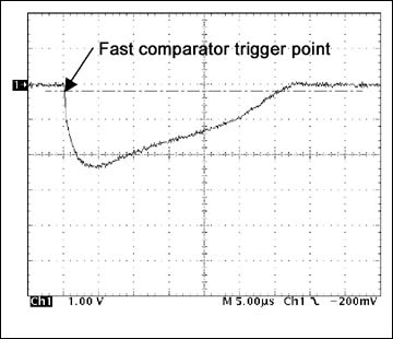
Figure 5. The circuit has 400A peak short-circuit current without modification
Observing the voltage signal waveform shown in Fig. 6 is helpful for deepening understanding. The figure shows the output voltage during short circuit, the M1 gate voltage waveform, and the voltage across RS. All voltages are referenced to + 12V input.
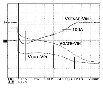
Figure 6. Short-circuit voltage and current waveforms without circuit modification
The VOUT-VIN signal waveform shows that VOUT dropped by 7V during the short circuit, which indicates that the short circuit impedance is only slightly lower than ½ of the total circuit impedance. Short-circuit faults with lower impedance will produce peak currents above 400A. The signal waveform also shows that the short circuit is not completely reliable within the first 300 ns; this causes the VSENSE signal waveform to fall slowly.
It can be seen from the VGATE waveform that initially VGS = 7V. Due to the decrease of VOUT, it increased to about 10V after 1µs. VGS only drops to 9V after 5µs, 6V at 20µs, and 4V at 33µs. Since the discharge current is only 3mA, the gate discharge is slow. In this way, the short-circuit current is still 100A within 27µs after a short-circuit fault occurs.
The fast gate pull-down circuit in Figure 2 does not reduce the initial short-circuit current, but the PNP Darlington tube pull-down will quickly terminate the current signal waveform. The short-circuit current signal waveform in this configuration is shown in Figure 7. The peak current is still 2400mV or 400A, but after the fast comparator is triggered at 370ns, the current can be blocked within 50ns. It should also be noted that the short circuit current signal waveform is very steep, indicating that the mechanical short circuit is very reliable.
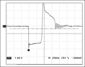
Figure 7. Short-circuit current waveform of fast pull-down circuit
When the circuit capacitor charges the input capacitor, the supply current reverses and causes a small positive overshoot at the + 12V input.
The fast short-circuit peak current limiting circuit of FIG. 3 is effective in limiting the peak current and the duration of the short-circuit current. As shown in Figure 8, the peak voltage across RS (6mΩ) is 600mV, which corresponds to a peak current of 100A. Short-circuit current blocking is extremely rapid, and the current pulse is completely terminated within 200ns.
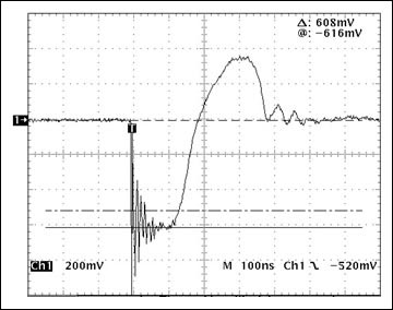
Figure 8. Short-circuit current pulse of the improved hot-swap controller circuit
Using this technology can minimize the backplane power supply interference. As shown in Figure 9, the peak voltage interference of less than ± 500mV will be generated on the + 12V power supply mentioned in the test method section.
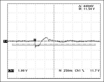
Figure 9. Backplane interference caused by a short circuit in Figure 3
Seeing the steep current wavefront again indicates that this is a very high-quality short-circuit condition. Unfortunately, it is difficult to reproduce such a steep current waveform. So what happened? The PNP-NPN detection / pull-down circuit terminated the short-circuit current (and then released the control) so quickly that the MAX4272 fast comparator did not have enough time to trigger (response time = 350ns). Figure 10 shows the VGS signal waveform in the 500µs period (450µs after the short circuit starts). Since the 100µA gate charging current still exists, the gate voltage that has been discharged begins to rise again. After about 130µs, the gate voltage is fully charged (3V) and VOUT rises to about 1V, at which time the short-circuit current begins to flow again. The recharging process is slow enough to allow the fast comparator to trigger at a current of 33A (200mV / 6mΩ), and the IC will perform a shutdown and latch operation.
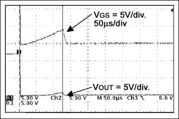
Figure 10. Time-compressed view of VGS under short-circuit conditions. Conclusion When the hot-swap control circuit has a short-circuit fault, both circuits discussed in this article can protect the backplane power supply by limiting power consumption. The simple circuit shown in Figure 2 can shorten the duration of the short-circuit current to less than 500ns; the circuit of Figure 3 is slightly more complicated, but the short-circuit current can be limited to less than 100A, and the pulse width of the short-circuit current is less than 200ns.
Any of the above technologies are suitable for most hot-swap control circuits.
Depending on the internal resistance of the power supply, the short-circuit impedance, the characteristics of the short-circuit fault itself and the time when the fault occurs, there will be some differences in individual test results.
This application note presents a simple external circuit that minimizes the initial current spike and isolates short-circuit faults within 200 to 500ns.
Typical hot-swap circuit Let's examine the + 12V, 6A typical hot-swap control circuit built with MAX4272 (Figure 1). According to the specifications of the MAX4272, it can be seen that it includes low-speed and fast comparators with trigger thresholds of 50mV and 200mV respectively (over the entire temperature range, tolerances are 43.5mV to 56mV and 180mV to 220mV, respectively). The trigger current is usually 1.5 to 2.0 times the operating current, select RSENSE = 5mΩ. RSENSE allows a tolerance of 5%. The trigger current range of the low-speed comparator under overload conditions is 8.28 to 11.76A; when a short circuit occurs, the trigger current range of the fast comparator is 34A to 46.2A.

Figure 1. Typical hot-swap control circuit
The minimum trigger threshold of the low-speed comparator is 38% higher than the normal operating current, and the short-circuit trigger threshold of the fast comparator is 6 to 8 times the operating current.
The delay time of the fast comparator is 350ns, and the short-circuit current spike during this period is limited only by the circuit impedance. After that, the current slowly decreases until the short-circuit fault is completely isolated. The 3mA gate pull-down current limits the discharge rate of the MOSFET M1 gate capacitance (3nF to 4nF). The short-circuit current slowly decreases from 15µs to 40µs, and at the same time, the gate voltage is pulled from 19V to near ground potential. Peak short-circuit current The initial peak current within 350ns is determined by the following factors:
(a) Power supply ESR, (b) Short-circuit state, (c) RSENSE resistance, (d) M1 RDS (ON), (e) M1 ID (ON).
The above parameters adopt the values ​​closest to the actual situation, and the total impedance of the circuit during short circuit can be calculated:
(Power supply ESR ≈ 4mΩ) + (Short circuit ≈ 3mΩ) + (RSENSE = 5mΩ) + (RD (ON) ≈ 4mΩ) ≈ 16mΩ.
At this time, the short-term peak current is: ISC ≈ 750A, and depends on the energy storage capacitor of the power supply (when the low ESR backplane with a 2200µF capacitor is discharged at 750A, the voltage within 1µs will only decrease by 340mV). In this case, the actual peak ISC will be limited to about 400A by M1's ID (ON).
ID (ON) depends on VGS, so it is necessary to check the circuit to determine the gate-source voltage during this period. The MAX4272 includes an internal charge pump that allows the gate voltage during normal operation to be about 7V higher than VIN. Therefore, when the MOS tube is turned on, VGS = 7V.
The second effect of the short circuit is that it actually increases VGS. The short circuit introduces a voltage step between the drain and source of M1-equal to a part of the total input voltage. Since the RD (ON) of M1 is about 1/3 of the estimated total impedance of the short circuit, the VDS applied at this time is about 1/3 of the 12V step voltage. The voltage divider composed of the drain-gate capacitance cdg and the gate-source capacitance cgs will transfer a part of this step voltage to the gate. After proper calculations, it can be seen that the additional ΔVGS introduced is 300mV to 500mV, but tests conducted during the short circuit show that this value can be as high as ΔVGS = + 3V.
At this point, it can be clearly seen that a solid and reliable short circuit can generate hundreds of amperes of current in a few microseconds to tens of microseconds.
Designers may wish to limit the peak ISC to 50A for a duration of less than 1µs, but this requirement is impractical without adding faster comparators and gate pull-down circuits. However, some simple modifications to the circuit can be considered. During the initial 350ns response time of the internal fast comparator, the current will be limited to a few hundred amperes by ID (ON). In this case, a simple external circuit can be added to speed up the gate discharge, thereby limiting the short circuit duration to ≤ ½µs . Or use a slightly more complicated external circuit to limit the peak Isc to 100A, and the duration is ≤ 200ns. The fast gate pull-down circuit limits the duration of the large short-circuit current by simply adding a PNP Darlington tube Q1, which can greatly shorten the duration of the large short-circuit current, as shown in Figure 2. Diode D1 allows the gate to charge normally in the on state, while the controller discharges the 3mA gate discharge current to directly drive the base of Q1 when it is off. Then Q1 quickly completes the gate discharge in about 100ns. In this way, the duration of the large current when the short circuit occurs is greatly shortened, which is only slightly longer than the 350ns delay time of the fast comparator.

Figure 2. Hot-swap controller with fast gate pull-down. Fast current limiting circuit With the circuit shown in Figure 3, the short-circuit current can be limited to less than about 100A for a duration of less than 200ns. When the voltage difference across RSENSE reaches about 600mV, the PNP transistor Q1a will trigger and drive the NPN transistor Q1b, thereby quickly discharging the gate capacitance of M1.

Figure 3. Hot-swap controller with fast short-circuit peak current limit
C2 between the gate and source of M1 can further reduce the forward transient step voltage applied to the gate when a short circuit occurs. The value of this capacitor ranges from 10nF to 100nF.
Zener diode D1 is used to limit VGS to a value below 7V (MAX4272 provides this voltage).
Although the Zener diode D1 is rated at 5.1V at a bias current of 5mA, in this circuit, the MAX4272 can only output a gate charge current of 100µA (Zener diode bias current), so D1 limits VGS At about 3.4V. Restricted VGS can reduce ID (ON), and of course RD (ON) will increase. According to the data of MOS tube: RD (ON) is 5mΩ when VGS is 3.4V, and RD (ON) is 3mΩ when VGS is 7V. This can turn off M1 faster.
D1 and C2 can also be used in the circuits of Figure 1 and Figure 2 to reduce the ID (ON) during short circuit. Test Method-There is nothing easier to create a short circuit than to make a short circuit.
However, it is very challenging to produce a reliable, reliable, and repeatable short circuit. This test evaluates the following methods of making short circuits. When the mechanical switch is closed, there will always be a few milliseconds of contact vibration process. Rotary multi-contact switches seem to avoid similar situations, but because the electric sparks formed by multiple large current closures will corrode the contacts, the repeatability of the switch is doubtful. High-current relay contacts also produce jitter when closed, and will exhibit different closing resistances. The experiment proves that the current rising rate of the thyristor is not satisfactory. High-current mercury displacement relays are the best method people have high hopes, but the results are not satisfactory. A 60A, 600V mercury relay with a nominal impedance of 4mΩ has an impedance of 40mΩ at the beginning of contact, and will easily drop to 4mΩ as the current pulse flows for 15µs. Manual short-circuit operation can provide a random, intermittent and non-repetitive shorting method, with strong randomness! A very steep current wave front can be obtained. In summary, although contact corrosion has an impact on the repeatability of each closure, this method is still the most effective (and most economical). The most feasible laboratory method is to use multiple large output CMOS Schmitt line drivers to drive multiple parallel, low RD (ON), NMOS transistors. Due to time and resource constraints, this option was not adopted.
It is extremely difficult to consistently produce true low-resistance short-circuit faults with steep current fronts by mechanical means in the laboratory. The circuit will almost certainly experience this unexpected short-circuit fault when it is in operation.
Usually artificial short circuit will produce the capacitor discharge current and voltage waveform as shown in Figure 4. The upper curve is the short-circuit output voltage recorded when 5V / div is selected. It can be seen that most of the time (25µs / div) the capacitor discharges less than half. The lower curve is the short-circuit current recorded when the 25A / div gear is selected, which clearly shows that the contact is intermittent.

Figure 4. Irregular mechanical short circuit signal waveform
It is not easy to construct a power supply with an ESR lower than 5mΩ. Despite this, every effort has been made to construct a low ESR (4-5mΩ) voltage source. After careful measurement, it can be seen that the voltage drops by 440mV in the case of a 100A short circuit. The input of the voltage source is directly connected in parallel with a 5500µF computer-grade electrolytic capacitor, a 3.3µF multilayer ceramic capacitor and six 100µF professional polymer aluminum electrolytic capacitors, and is driven by a 10A power supply. The short-circuit current waveform of the circuit shown in Fig. 1 (without improvement) is shown in Fig. 5. Since the voltage across the current-sense resistor RS is measured and the oscilloscope ground is connected to the + 12V input of the test circuit, the signal waveform appears to be inverted. RS is 6mΩ, the voltage range is 1V / div, and the peak voltage is 2400mV or 400A. The current wavefront is not as steep as when it is in good contact.

Figure 5. The circuit has 400A peak short-circuit current without modification
Observing the voltage signal waveform shown in Fig. 6 is helpful for deepening understanding. The figure shows the output voltage during short circuit, the M1 gate voltage waveform, and the voltage across RS. All voltages are referenced to + 12V input.

Figure 6. Short-circuit voltage and current waveforms without circuit modification
The VOUT-VIN signal waveform shows that VOUT dropped by 7V during the short circuit, which indicates that the short circuit impedance is only slightly lower than ½ of the total circuit impedance. Short-circuit faults with lower impedance will produce peak currents above 400A. The signal waveform also shows that the short circuit is not completely reliable within the first 300 ns; this causes the VSENSE signal waveform to fall slowly.
It can be seen from the VGATE waveform that initially VGS = 7V. Due to the decrease of VOUT, it increased to about 10V after 1µs. VGS only drops to 9V after 5µs, 6V at 20µs, and 4V at 33µs. Since the discharge current is only 3mA, the gate discharge is slow. In this way, the short-circuit current is still 100A within 27µs after a short-circuit fault occurs.
The fast gate pull-down circuit in Figure 2 does not reduce the initial short-circuit current, but the PNP Darlington tube pull-down will quickly terminate the current signal waveform. The short-circuit current signal waveform in this configuration is shown in Figure 7. The peak current is still 2400mV or 400A, but after the fast comparator is triggered at 370ns, the current can be blocked within 50ns. It should also be noted that the short circuit current signal waveform is very steep, indicating that the mechanical short circuit is very reliable.

Figure 7. Short-circuit current waveform of fast pull-down circuit
When the circuit capacitor charges the input capacitor, the supply current reverses and causes a small positive overshoot at the + 12V input.
The fast short-circuit peak current limiting circuit of FIG. 3 is effective in limiting the peak current and the duration of the short-circuit current. As shown in Figure 8, the peak voltage across RS (6mΩ) is 600mV, which corresponds to a peak current of 100A. Short-circuit current blocking is extremely rapid, and the current pulse is completely terminated within 200ns.

Figure 8. Short-circuit current pulse of the improved hot-swap controller circuit
Using this technology can minimize the backplane power supply interference. As shown in Figure 9, the peak voltage interference of less than ± 500mV will be generated on the + 12V power supply mentioned in the test method section.

Figure 9. Backplane interference caused by a short circuit in Figure 3
Seeing the steep current wavefront again indicates that this is a very high-quality short-circuit condition. Unfortunately, it is difficult to reproduce such a steep current waveform. So what happened? The PNP-NPN detection / pull-down circuit terminated the short-circuit current (and then released the control) so quickly that the MAX4272 fast comparator did not have enough time to trigger (response time = 350ns). Figure 10 shows the VGS signal waveform in the 500µs period (450µs after the short circuit starts). Since the 100µA gate charging current still exists, the gate voltage that has been discharged begins to rise again. After about 130µs, the gate voltage is fully charged (3V) and VOUT rises to about 1V, at which time the short-circuit current begins to flow again. The recharging process is slow enough to allow the fast comparator to trigger at a current of 33A (200mV / 6mΩ), and the IC will perform a shutdown and latch operation.

Figure 10. Time-compressed view of VGS under short-circuit conditions. Conclusion When the hot-swap control circuit has a short-circuit fault, both circuits discussed in this article can protect the backplane power supply by limiting power consumption. The simple circuit shown in Figure 2 can shorten the duration of the short-circuit current to less than 500ns; the circuit of Figure 3 is slightly more complicated, but the short-circuit current can be limited to less than 100A, and the pulse width of the short-circuit current is less than 200ns.
Any of the above technologies are suitable for most hot-swap control circuits.
Depending on the internal resistance of the power supply, the short-circuit impedance, the characteristics of the short-circuit fault itself and the time when the fault occurs, there will be some differences in individual test results.
Premium and Atrium PLCs offer main counting functions (down-counting, upcounting, up/down counting) from the application-specific "counting" modules ("Installing the Counting Module", Premium and Atrium using PL7, Counter modules, User manual). Three modules are offered: z a 2-channel module and a 4-channel module for the incremental encoder, with a maximum reading frequency of 40 kHz, z a 2-channel module for: z incremental encoder, with a maximum reading frequency of 500 kHz, z absolute SSI series encoder, with a maximum reading frequency of 2 MHz.
Modicon Premium PLC,Schneider Communication Module,Modicon SRAM Memory Cards,Modicon PLC Processors
Xiamen The Anaswers Trade Co,.LTD , https://www.answersplc.com