The development of science and technology has surpassed our imagination, and the innovation of technology continues to scream us. Looking back on 2017, we can see that nano-scale LEDs break through the inter-chip transfer rate limit, the world's first 72-layer 3D NAND comes out, and the emergence of a series of technologies such as 1nm process manufacturing, to write a new chapter for the future. In this context, Electronic Enthusiasts has compiled ten of the latest technological breakthroughs for readers to understand the most cutting-edge trends in the electronics industry.
First, graphene has made a major breakthrough in building OLED electrodes.
At the beginning of January 2017, researchers made OLED electrodes through graphene, which also opened the curtain for the development of graphene in the OLED industry. It is understood that graphene has the characteristics of high image quality, flexible ultra-thin, high contrast, low energy consumption, etc. It can create excellent touch panel materials with excellent hardness, excellent electrical conductivity, flexible touch and super transparency. This time, researchers used graphene to create OLED electrodes, which is a major breakthrough.

According to experts, the size of the electrode attached to the OLED is about 2 cm x 1 cm, which is fabricated using a chemical vapor deposition (CVD) process in which methane and hydrogen are pumped into a vacuum chamber and the copper plate is heated to 800 °C. These two gases undergo a chemical reaction and form a graphene atom on the surface when methane is dissolved in the copper. Once the layer is fully formed, the entire device is allowed to cool, a protective polymer sheet is applied, and then copper is chemically etched away to reveal a monoatomic layer of pure graphene.
Dr. Beatrice Beyer, head of the FEP project at Fraunhofer's organic electronics, electron beam and plasma technology, said, “This is a real breakthrough in the research and integration of extremely demanding materials. Although this is not the first flexible display that uses graphene in its construction. But it introduces OLED technology for the first time, taking a big step toward full-color screens and fast response times."
China Graphene Industry Alliance said that the annual global graphene production capacity will reach 100 tons, and will reach 1,000 tons in the next 5-10 years. By 2020, the global graphene market will exceed 100 billion yuan.
Second, China's 5nm carbon nanotube CMOS device research new breakthrough
On January 20th, Pei Lianmao and Zhang Zhiyong of the School of Information Science and Technology of Peking University made a world-class breakthrough in the field of carbon nanotube electronics: the first preparation of high-performance carbon nano-transistors with 5 nm gate length, and proved its performance beyond Equal-sized silicon-based CMOS (complementary metal-oxide-semiconductor) field effect transistors push transistor performance to the theoretical limit.
It is understood that the group achieved the first sub-threshold swing of p-type and n-type devices by optimizing the device structure and fabrication process for the first time to achieve a carbon nanotube top-gate CMOS field effect transistor with a gate length of 10 nm (corresponding to a 5 nm technology node). (subthreshold swing, SS) are 70mV/DEC.
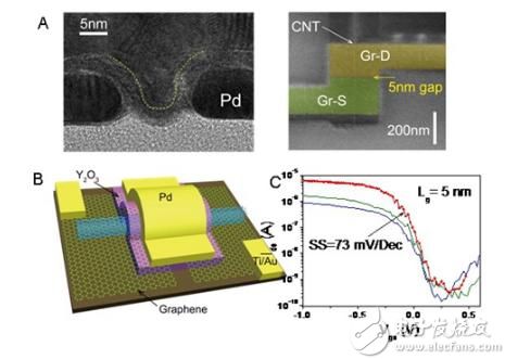
5nm gate length carbon nanotube transistor (A, cross-section transmission electron micrograph of metal-contacted carbon tube transistor, and scanning electron micrograph of carbon nanotube transistor using graphene as contact; B, schematic diagram of graphene as contact carbon tube transistor; C, 5nm Transfer curve of gate long carbon nanotube transistor)
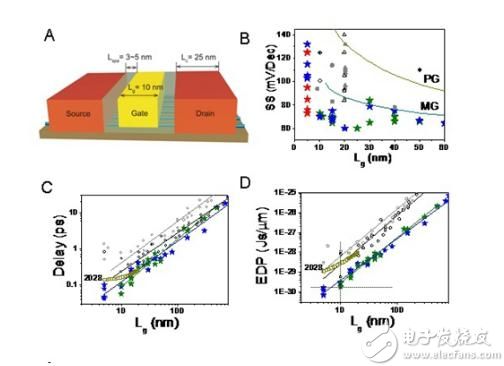
Comparison of Carbon Tube CMOS Devices and Conventional Semiconductor Devices (A, Schematic Diagram of Field Effect Transistor Based on Carbon Tube Array, Comparison of BD, Carbon Tube CMOS Devices and Traditional Material Transistors)
Device performance not only far exceeds all published carbon nanotube devices, but at lower operating voltages (0.4V), both p-type and n-type transistors outperform the best (Intel's 14nm node) silicon-based The performance of CMOS devices operating at 0.7V. The intrinsic gate delay of a special carbon nanotube CMOS transistor is 0.062 ps, which is equivalent to 1/3 of a 14 nm silicon-based CMOS device (0.22 ps).
At the same time, the research team also studied the effect of contact size reduction on device performance, explored the reduction of the overall size of the device, and reduced the contact electrode length of the carbon tube device to 25 nm. Under the premise of ensuring device performance, the overall size was 60 nm. The carbon nanotube transistor has successfully demonstrated a carbon nanotube CMOS inverter with an overall length of 240 nm, which is the smallest nano-inverter circuit currently implemented.
Third, nano-scale LED breakthrough chip-to-chip transfer rate limit
In mid-February, researchers at the Eindhoven University of Technology in the Netherlands published the latest research on on-chip waveguide-coupled nanocolumn metal cavity LEDs in the journal Nature Communications. The researchers demonstrated a nanoscale LED layer stack bonded to a silicon substrate and coupled to an indium phosphide (InP) thin film waveguide to form a shutter coupler.
It is understood that this nano-LED adopts the sub-micron nano-column shape, which is 1000 times more efficient than the previous generation components, and the output power at room temperature is only a few nanowatts (nW), compared with the previous research results. Approximately picowatt (pW) grade output power. According to the research paper, this component is capable of exhibiting a relatively high external quantum efficiency. At low temperatures, the researchers released a power stage of 50nW, which is equivalent to transmitting more than 400 photons per bit at 1Gb/s, which is much higher than the ideal noise limit of the ideal receiver. The component operates at a telecom wavelength (1.55μm) and can be modulated by a pulse waveform generator with a frequency up to 5GHz.
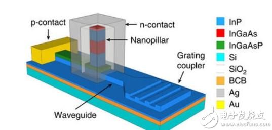
Schematic diagram of nano-columnar LED on silicon substrate
Researchers say that because of the low loss of short-distance interconnects and the continued advancement of integrated receiver technology, this power stage is expected to enable data transfer within the chip with ultra-compact light sources.
Researchers have also developed a surface passivation method that can further increase the efficiency of nano-LEDs by a factor of 100 while further reducing power consumption by improving ohmic contacts.
Fourth, help power communication development, China developed a hundred millisecond high efficiency quantum memory
Professors Jian Jianwei and Bao Xiaohui of the University of Science and Technology of China have used the cold atom ensemble to develop the 100-millisecond high-efficiency quantum memory for the first time in the world, laying a solid foundation for the construction of long-distance quantum relay systems. This achievement has been published in the international authoritative academic journal Nature and Photonics.
The so-called quantum communication refers to a new type of communication method that uses the quantum entanglement effect to transmit information. After more than 20 years of development, the discipline of quantum communication has gradually moved from theory to experiment and to practical development. The main fields involved include: quantum cryptography communication, quantum remote transmission and quantum dense coding. Quantum communication is characterized by high efficiency and absolute security, and is currently a research hotspot in international quantum physics and information science.
In recent years, network security issues have been receiving much attention from the world, and various network security incidents have frequently occurred. With the development of events such as the “Prism Gate†and changes in the global political situation, information security has attracted the attention of all countries in the world. The advent of quantum communication systems has solved the problem of cybersecurity in the future quantum computing era. In the field of quantum security communication applications, China is at the forefront of the world.
In 2012, Chinese scientists and professors of the Chinese University of Science and Technology Pan Jianwei and others successfully achieved the first free-space quantum teleportation and entanglement distribution of the hundred-kilometer level in the world, and developed a millisecond-level efficient quantum memory for launching the world's first "quantum communication satellite." "laying the technical foundation." On August 16, 2016, the world's first quantum science experimental satellite "Mozi", which was independently developed by Chinese scientists, was launched and will realize quantum communication between satellite and ground for the first time in the world.
However, the storage time of the memory developed in 2012 is still far from the actual demand of the remote quantum relay. In recent years, Pan Jianwei team developed a number of key experimental techniques such as three-dimensional optical lattice limiting atomic motion, which greatly reduced the decoherence caused by atomic motion, and finally achieved a storage life of 0.22 seconds and a read efficiency of 76%. High performance quantum memory.
5. The Japanese research team produced high-quality 2-inch GaN chips and MOSFETs.
The joint team of Mitsubishi Chemical and Fuji Electric, Toyota Central Research Institute, Kyoto University, and Industrial Technology Research Institute successfully solved the key technologies for forming GaN component power semiconductors on gallium nitride (GaN) chips. GaN power semiconductors are the next generation technology for silicon carbide power semiconductors. Japan has accumulated GaN component technology through the development of light-emitting diodes, and GaN chip production accounts for the highest share in the world. If the existing technology is put into practical use, it will be in a dominant position in the world.
Power semiconductors are conducive to energy conservation in home appliances, automobiles, and electric vehicles, and the industrial demand is large. In GaN power semiconductors, devices such as high-electron mobility transistors with horizontal GaN-based transistors on silicon substrates have been mass-produced. However, research on high-performance devices for metal-oxide-semiconductor field-effect transistors (MOSFETs) for forming GaN on GaN substrates has just started. . The United States is also actively studying and the world is fiercely competitive in development.
The Japanese team produced high quality 2-inch GaN chips and MOSFETs. Mitsubishi Chemical has improved the "Ammonia Thermal Method" for GaN chip mass production technology for power semiconductors. Optimize the crystal growth conditions and reduce the average defect density of the chip to a few hundredths of the previous level and thousands of levels per square centimeter. Their 2018 goal is to further reduce defects by more than one digit to achieve a 4-inch large chip.
Sixth, SK hynix launched the world's first 72-layer 3D NAND
On April 11, SK hynix officially announced the world's first 72-layer 256Gb 3D NAND flash memory based on TLC arrays. This is another major breakthrough for SK hynix after the announcement of the first 48-layer 3D NAND chip in November 2016, just five months later.
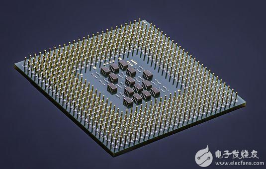
According to reports, compared to the previously introduced 48-layer 3D NAND chip, the 72-layer chip has increased the number of units by 1.5 times and the production efficiency has increased by 30%. At the same time, thanks to the high-speed circuit design, the internal operating speed of the 72-layer chip has doubled to 48 chips, and the read/write performance has increased by 20%.
SK Hynix said that 72-layer 3D NAND chips will be mass-produced in the second half of this year to meet the demand for high-performance SSDs and smartphone devices.
Seven, American researchers announced the realization of 1nm process manufacturing
In early May, researchers at the Brookhaven National Laboratory, part of the US Department of Energy (DOE), announced the creation of a new world record. They successfully manufactured printing equipment measuring only 1 nm in size, using electron beam printing instead of traditional ones. Lithographic printing technology.
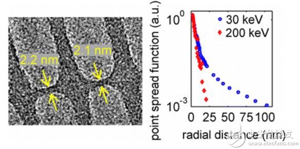
The researchers in this laboratory have creatively used electron microscopy to create smaller sizes than conventional EBL (electron beam printing) processes, and electronically sensitive materials are greatly reduced in size by focusing electron beams. The point at which a single atom can be manipulated. The tool they created can dramatically change the properties of a material, from conduction to light transmission and interaction in both states.
Their achievement was done at the Center for Functional Nanomaterials under the Department of Energy, and STEM (Scanning Projection Electron Microscopy) was used for 1nm printing, separated by 11nm, so that 1 trillion features per square millimeter can be achieved. The density of points. A 2 nm resolution was achieved with a bias correction STEM at a 5 nm half gate under a hydroxide silicate resist.
In fact, this is not the first time that scientists have achieved the 1nm process. Last year, the US Department of Energy's other national laboratory, Lawrence Berkeley National Laboratory, also announced the 1nm process. They used carbon nanotubes and molybdenum disulfide. Wait for new materials. Similarly, this technology will not be put into mass production very soon, because carbon nanotube transistors are similar to PMMA and electron beam lithography here, and the current semiconductor technology is obviously different. This is simply impossible.
Eight, scientists create the "world's thinnest" nanowires
In late May, researchers at Cambridge and Warwick University successfully produced the “world's thinnest†nanowires (shrinking wires to the width of a single atomic string) by injecting carbon nanotubes through tellurium.
In fact, in the three-dimensional (3D) world, there is no pure one-dimensional (1D) or two-dimensional (2D) material. Even if it is a thin piece of paper, it is thick, but to simplify thinking, we can think of the monoatomic layer of graphene as only length and width.
This "one-dimensional extreme nanowire" concept has something in common with two-dimensional graphene materials. It is made of tantalum elements and is only a single atom wide and tall. But for stability reasons, the researchers still "blocked" it in carbon nanotubes.
However, this single-atom microscale also brings some problems, such as the atom often deducts behaviors that are inconsistent with the scientists' assumptions. In addition, if there is no structural constraint, the one-dimensional material is easily decomposed.

According to paper author Paulo Medeiros, when dealing with such a small material, it is usually necessary to place it on a surface. The problem is that these surfaces are usually electrically resistant. However, carbon nanotubes are chemically quite inert, and can not only fix such a one-dimensional structure, but also affect its conductivity. This is just the beginning of our systematic understanding of the physical and chemical properties of one-dimensional materials. There are still many basic physics knowledge waiting for us to uncover.
In addition, the team also found that by changing the diameter of the nanotubes, they were able to control other properties of the crucible. Typically, this element is a semiconductor. But under strict restrictions, its behavior is more like a metal.
Nine, Apple announced a new patent Bluetooth sensor car can communicate with each other
On August 21, Apple announced the latest patent, which uses sensor technology to help communicate with each other. The sensor's technology is similar to Bluetooth short-range wireless communication, which scans the surrounding environment of the vehicle and transmits data to other vehicles, sensors and GPS.
It is understood that Apple's sensor is similar to Bluetooth short-range wireless technology, which can scan the surrounding environment, communicate with other cars, sensors and GPS systems, and update the driver's dashboard display to remind drivers to gallop on the road. And the vehicle or ambulance. Apple did not say that the technology would be used in the field of autonomous driving, but rather described it as an enhanced version of the parking sensor and blind spot detection system, which have been commonly used in automobiles.
The communication between cars is nothing new. As early as 2002, Auto Communication Alliance Broadcom has been studying this technology, and Qualcomm has similar solutions.
Apple’s patent for Bluetooth sensors is now meaningful, and Apple’s CEO Cook said “is investing heavily in building automated systems, one of the main applications being cars.†Apple’s improved mobile operating system, CarPlay, is designed In the car. As autonomous vehicles take on more of the driver's traditional responsibilities, systems like CarPlay may be more widely used.
Ten, Qualcomm launched the first 5G modem chipset
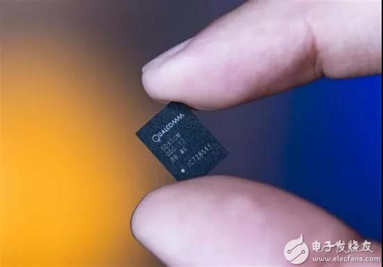
On October 17, Qualcomm announced the official launch of its first 5G modem chipset for mobile devices in Hong Kong and successfully demonstrated the world's first 5G data connection to mobile devices. At the same time, Qualcomm also demonstrated the first 5G smartphone reference design for next-generation cellular connectivity.
Qualcomm's test was conducted at the Qualcomm Technologies lab in San Diego, and experiments have shown that Qualcomm's Opteron X50 NR modem chipset has achieved gigabits per second download speed over multiple 100 MHz 5G carriers, which is now more than now Smartphones on 4G LTE wireless networks can download several times faster. At the same time, Qualcomm also completed the data connection in the 28GHz millimeter wave band. At present, the Qualcomm X50 5G baseband only supports the 28GHz mmWave millimeter wave specification, and only the two operators of South Korea KT and US Verizon support.
To demonstrate the 5G data connectivity of mobile devices, Qualcomm also brought the first 5G smartphone as a reference design. It is reported that this phone uses a comprehensive screen design, front fingerprint, support for fingerprint recognition under the screen, rear dual camera, thickness of 9mm. Qualcomm said that 5G smartphones and networks will be commercially available in the first half of 2019, and 5.2 years of debugging time will be required for 5G baseband, RF, and network.
Cristiano Amon, Executive Vice President of Qualcomm, said: "This important milestone and our 5G smartphone reference design fully demonstrate that Qualcomm Technologies is driving the development of 5G new airspace in the mobile terminal space to enhance the mobile broadband experience for consumers worldwide."
In fact, last year Qualcomm released the world's first 5G baseband solution "Snapdragon X50 5G Modem", and at the Qualcomm 5G summit in February, it has announced the completion of the 5G new radio (New Radio), and is expected to meet in 2018 Related equipment is available.
In addition to Qualcomm, Intel, Apple, Huawei and other manufacturers are pushing the 5G revolution. 5G technology will likely become the basis for the future popularity of IoT technology. According to Li Weixing, vice president of Qualcomm's QCT technology, 5G technology is expected to be used in energy management, wearable devices, networked medical, object tracking and environmental monitoring.
Our company specializes in the production and sales of all kinds of terminals, copper terminals, nose wire ears, cold pressed terminals, copper joints, but also according to customer requirements for customization and production, our raw materials are produced and sold by ourselves, we have their own raw materials processing plant, high purity T2 copper, quality and quantity, come to me to order it!
Cable Terminals
Taixing Longyi Terminals Co.,Ltd. , https://www.longyicopperterminals.com