0 Preface
Medical power supply is a device with high safety regulations, EMI and EMC. As a green switching power supply, it will bring huge changes to human society in the 21st century. A medical device system with excellent performance cannot be separated from a control module with excellent performance, and the performance of the control module depends to a large extent on the performance of the power supply, so a high-quality power supply system occupies a very important position in the entire medical system. This article is based on UC3842 high-performance current mode PWM generator controlled switching power supply suitable for such systems. This design achieves complete isolation of output and input through a small high-frequency transformer, which not only improves the efficiency of the power supply, simplifies the peripheral circuit, but also reduces the cost and volume of the power supply. The output voltage of the power supply is stable, the ripple is small, the uninterrupted performance is reliable, and it will not cause radiation and conduction interference to other equipment.
1 The basic structure of a single-ended flyback converter circuit
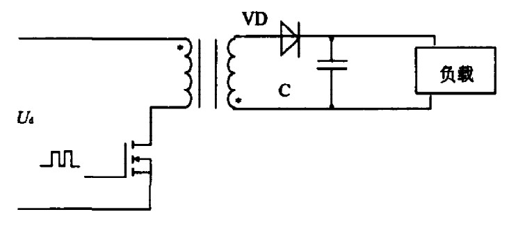
The typical structure of single-ended flyback conversion is shown in Figure 1. Single-ended means that the magnetic core of the transformer only works on one side of the hysteresis loop; flyback means that when the switch is turned on, energy is stored in the primary coil, while the secondary coil is not connected. When the switch is closed, the primary The energy in the coil is released to the load through the secondary coil. This is a low-cost regulator, which can completely isolate the input and output parts, and has a better voltage regulation rate.

Figure 1 Single-ended flyback converter
2 Performance characteristics of UC3842 chip
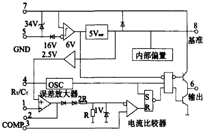
The UC3842 chip is a product of Unit Rode. It is a high-performance single-ended output current-controlled pulse width modulator chip. Its functional block diagram is shown in Figure 2. It consists of a 5V reference voltage source, an oscillator that controls duty cycle adjustment, a current measurement comparator, a PWM latch, a high-gain E / A error amplifier, and a large current push-pull output circuit suitable for driving power MOSFETs. Its main features are:
â‘ There are few external components, the peripheral circuit is simple, and the price is cheap;
â‘¡No input transformer is required, and the starting current is small (less than 1mA);
③With a precise voltage reference source (± 1%);
â‘£High current (1A) PWM output stage, can directly drive the power MOS tube;
⑤With under voltage blocking and over current protection functions;
â‘¥ Working frequency can reach 500kHz.

Figure 2 VC3842 principle block diagram
UC3842 chip can meet both good electrical performance and low cost, so it is widely used in small power switching power supply of 20 ~ 80W. Pin 2 in Figure 2 is its internal reference voltage (5V); Pin 7 is its power supply terminal, the chip operating start voltage is 16V, and the undervoltage lockout voltage is 10V; Pin 4 is connected to the oscillation circuit to generate a sawtooth wave RT of the required frequency Connect between pin 4 and pin 8, CT connect between pin 4 and ground. Pins 1 and 2 are the compensation input and the inverting input of the internal voltage comparator. The current feedback signal introduced from pin 3 is compared with the voltage error signal of pin 1 to generate a PWM (pulse width modulation) wave from pin 6 (output End) output this signal to control the power device on and off. Pin 3 is the current detection input terminal. Because the input of the current comparator is set with a current clamp of 1V, when the current is too large and the voltage on the current detection resistor R9 (as shown in Figure 3) exceeds 1V (that is, the level of pin 3 is greater than 1V), it will be turned off. PWM pulse, so as to achieve the purpose of overcurrent protection.
A tablet computer is an electronic device that integrates mobile commerce, mobile communication and mobile entertainment, with a touch recognition LCD screen, handwriting recognition and wireless network communication functions. At present, the tablet computer has become the most popular electronic product.
1.In appearance, the tablet computer looks like a large-screen mobile phone, or more like a separate LCD screen.
2.In terms of hardware configuration, a tablet computer has all the hardware devices of a traditional computer, and has its own unique operating system, compatible with a variety of applications, and has a complete set of computer functions.
3.Tablet PC is a kind of miniaturized computer. Compared with traditional desktop computers, tablet computers are mobile and flexible. Compared with notebook computers, tablet computers are more compact and more portable.
4.Tablet PC is a digital notebook with digital ink function. In daily use, you can use the tablet computer like an ordinary notebook, take notes anytime and anywhere, and leave your own notes in electronic texts and documents.
Tablet Pc Pad,Mobile Tablet,Scratch Pad Tablet Pc,Tablet Pc,Tablets & Presentation Equipment,Educational Tablet
Jingjiang Gisen Technology Co.,Ltd , https://www.gisentech.com