Detailed description of the composition and principle of the switching power supply circuit
First, the circuit of the switching power supply The main circuit of the switching power supply is composed of input electromagnetic interference filter (EMI), rectifier filter circuit, power conversion circuit, PWM controller circuit, output rectifier filter circuit. The auxiliary circuit has an input over-voltage protection circuit, an output over-voltage protection circuit, an output over-current protection circuit, and an output short-circuit protection circuit.
The circuit block diagram of the switching power supply is as follows: 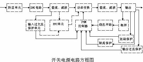
Second, the principle of the input circuit and common circuits
1, AC input rectifier filter circuit principle: 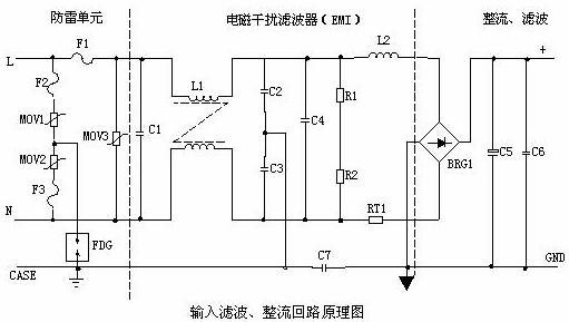
1 Lightning protection circuit: When there is lightning strike and high voltage is generated through the power grid, the circuit consists of MOV1, MOV2, MOV3: F1, F2, F3 and FDG1. When the voltage applied across the varistor exceeds its working voltage, its resistance decreases, so that the high-voltage energy is consumed on the varistor. If the current is too large, F1, F2, and F3 will burn and protect the latter circuit.
2 Input filter circuit: The double π-type filter network composed of C1, L1, C2 and C3 mainly suppresses the electromagnetic noise and clutter signals of the input power source to prevent interference to the power supply and also prevents high-frequency clutter generated by the power supply itself. Interference with the grid. When the power is turned on, the C5 should be charged. Because the instantaneous current is large, adding RT1 (thermistor) can effectively prevent the inrush current. Since the instantaneous energy is completely consumed on the RT1 resistor, the RT1 resistance decreases after the temperature rises after a certain time (RT1 is a negative temperature coefficient component), at which time the energy consumed is very small, and the latter circuit can work normally.
3 Rectifier filter circuit: After the AC voltage is rectified by BRG1, it is filtered by C5 to obtain a relatively pure DC voltage. If the C5 capacity becomes smaller, the output AC ripple will increase.
2, DC input filter circuit principle: 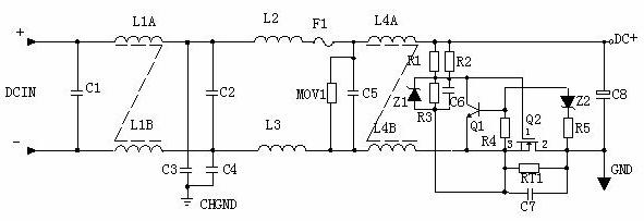
1 Input filter circuit: The double π-type filter network composed of C1, L1 and C2 mainly suppresses the electromagnetic noise and clutter signals of the input power source to prevent interference to the power supply, and also prevents high-frequency clutter generated by the power supply itself from the power grid. interference. C3 and C4 are safety capacitors, and L2 and L3 are differential mode inductors.
2 R1, R2, R3, Z1, C6, Q1, Z2, R4, R5, Q2, RT1, and C7 form an anti-surge circuit. At the moment of starting, due to the presence of C6, Q2 is not conducting, and the current forms a loop through RT1. Q2 turns on when the voltage on C6 is charged to the regulated value of Z1. If the C8 leakage or the short circuit of the latter stage is short, the voltage drop generated by the current on RT1 increases at the moment of starting, Q1 is turned on so that the gate voltage of Q2 is not turned on, and RT1 will burn out in a short time. Protect the rear stage circuit.
Third, the power conversion circuit
1. Working principle of MOS tube: At present, the most widely used insulated gate field effect transistor is MOSFET (MOS tube), which uses the electroacoustic effect of semiconductor surface to work. Also known as surface field effect devices. Since its gate is in a non-conducting state, the input resistance can be greatly improved up to 105 ohms. The MOS transistor uses the magnitude of the gate-source voltage to change the amount of induced charge on the semiconductor surface, thereby controlling the drain current. .
2, the common schematic: 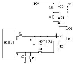
3. Working principle:
R4, C3, R5, R6, C4, D1, D2 form a buffer, and the switch MOS tube is connected in parallel, so that the voltage stress of the switch tube is reduced, EMI is reduced, and secondary breakdown does not occur. When the switch Q1 is turned off, the primary winding of the transformer is prone to spike voltage and spike current. These components combine to absorb the peak voltage and current well. The current peak signal measured from R3 participates in the duty cycle control of the current working cycle and is therefore the current limit of the current working cycle. When the voltage on R5 reaches 1V, UC3842 stops working and switch Q1 turns off immediately. The junction capacitances CGS and CGD in R1 and Q1 together form an RC network, and the charge and discharge of the capacitor directly affects the switching speed of the switching tube. If R1 is too small, it will cause oscillation and electromagnetic interference will be very large; if R1 is too large, it will reduce the switching speed of the switching tube. Z1 usually limits the GS voltage of the MOS transistor to 18V or less, thus protecting the MOS transistor. The gate controlled voltage of Q1 is saw-shaped wave. When the duty ratio is larger, the longer the Q1 conduction time is, the more energy the transformer stores. When Q1 is cut off, the transformer passes D1, D2, R5. R4 and C3 release energy and at the same time achieve the purpose of magnetic field reset, which is ready for the next storage and transmission of energy of the transformer. The IC adjusts the duty ratio of the 6-pin saw-wave according to the output voltage and current, thus stabilizing the output current and voltage of the whole machine. C4 and R6 are spike voltage absorption loops.
4. Push-pull power conversion circuit:
Q1 and Q2 will turn on in turn. 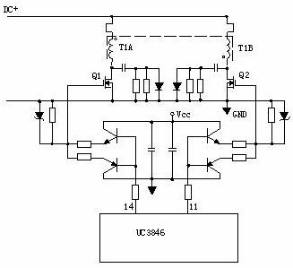
5. Power conversion circuit with drive transformer:
T2 is the drive transformer, T1 is the switching transformer, and TR1 is the current loop. 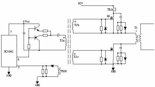
Fourth, the output rectifier filter circuit:
1. Forward rectifier circuit: 
T1 is a switching transformer whose phase of the primary and secondary poles is in phase. D1 is a rectifier diode, D2 is a freewheeling diode, and R1, C1, R2, and C2 are sharp peak circuits. L1 is a freewheeling inductor, and C4, L2, and C5 form a π-type filter.
2. Flyback rectifier circuit: 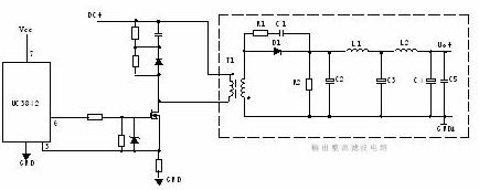
T1 is a switching transformer with opposite phases of the primary and secondary poles. D1 is a rectifier diode, and R1 and C1 are sharp peak circuits. L1 is a freewheeling inductor, R2 is a dummy load, and C4, L2, and C5 form a π-type filter.
3. Synchronous rectifier circuit: 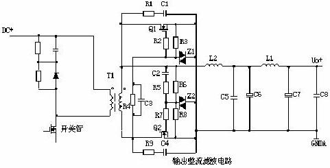
Working principle: When the upper end of the transformer is positive, the current is turned on by C2, R5, R6 and R7, the circuit forms the loop, and Q2 is the rectifier. The gate of Q1 is turned off due to the reverse bias. When the lower end of the secondary of the transformer is positive, the current is turned on by C3, R4, and R2, and Q1 is a freewheeling tube. The Q2 gate is turned off due to the reverse bias. L2 is a freewheeling inductor, and C6, L1, and C7 form a π-type filter. R1, C1, R9, and C4 are sharp peak circuits.
However, due to technical and cost reasons, it is not widely used. In recent years, RFID technology has developed by leaps and bounds. With the development of large-scale integrated circuit and network communication technology, RFID technology has entered the commercial application field, and began to develop from the initial low frequency (125kHz) and high frequency (13.56mhz) to uHF (860 ~ 960MHz) and microwave. RFID technology has become one of the most promising information technologies in the new era because of its unique advantages showing great development potential and application space. In both low and high frequency bands, China has independently developed RFID chips in accordance with ISO14443 A, B and ISO15693 standards, which have been successfully applied in major projects such as city bus all-in-one card and second-generation resident ID card. However, in the uHF and microwave field, China started late, technology and products are still relatively short. In this context, this paper studies the design of 915MHz rf card reader. The system can be applied to vehicle monitoring, remote control, telemetry, access control system, identity identification, non-contact radio frequency smart card, wireless 485/232 data communication, safety and fire prevention and other fields.
915MHZ Rubber Antenna ,915MHZ Antenna with magnetic base ,915MHZ fiberglass antenna
Yetnorson Antenna Co., Ltd. , https://www.xhlantenna.com