IGBT (Insulated Gate Bipolar Transistor), insulated gate bipolar transistor, is a composite fully controlled voltage-driven power semiconductor device composed of BJT (bipolar transistor) and MOS (insulated gate field effect transistor), which has both MOSFETs. The advantages of both the high input impedance and the low turn-on voltage drop of the GTR.

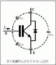
The IGBT combines the advantages of the above two devices, with low driving power and reduced saturation voltage. It is very suitable for converter systems with DC voltages of 600V and above, such as AC motors, inverters, switching power supplies, lighting circuits, traction drives, etc. Figure 1 shows an N-channel reinforced insulated gate bipolar transistor structure. The N+ region is called the source region, and the electrode attached to it is called the source. The N+ zone is called the drain zone. The control region of the device is the gate region, and the electrode attached thereto is called the gate. The channel is formed next to the boundary of the gate region. The P-type region (including the P+ and P regions) between the drain and the source (the channel is formed in this region) is called a Subchannel region. The P+ region on the other side of the drain region is called the Drain injector. It is a unique functional region of the IGBT. Together with the drain region and the sub-channel region, it forms a PNP bipolar transistor that acts as an emitter. The drain injects holes and conducts conductive modulation to lower the on-state voltage of the device. The electrode attached to the drain implant region is called the drain. The switching function of the IGBT is to form a channel by adding a forward gate voltage, and provide a base current to the PNP transistor to turn on the IGBT. Conversely, the reverse gate voltage is applied to eliminate the channel, and the base current is cut off to turn off the IGBT. The driving method of the IGBT is basically the same as that of the MOSFET. It only needs to control the input pole N-channel MOSFET, so it has high input impedance characteristics. When the channel of the MOSFET is formed, the hole from the P+ base is injected into the N layer (small sub-), and the N layer is conductance modulated to reduce the resistance of the N layer, so that the IGBT is also low at high voltage. On-state voltage.

The role of the gate resistor Rg 1. Eliminating the gate oscillation (or gate source) of the gate oscillating insulated gate device (IGBT, MOSFET) is a capacitive structure, and the parasitic inductance of the gate loop is inevitable, if not The gate resistance, which is a strong oscillation under the excitation of the driver drive pulse, must be connected in series to quickly attenuate. 2, the power loss of the transfer driver Capacitance inductance is a reactive component, if there is no gate resistance, the drive power will be mostly consumed in the output tube inside the drive, making its temperature rise a lot. 3. Adjusting the on-off speed of the power switching device The gate resistance is small, the switching device is fast on-off, and the switching loss is small; otherwise, it is slow, and the switching loss is large. However, if the driving speed is too fast, the voltage and current change rate of the switching device will be greatly increased, thereby causing a large interference, which will seriously make the entire device inoperable, and therefore must be balanced.

Phone Wireless Earphones,Sports Bluetooth Earphone,Best Cheap Wireless Earbuds,Wireless Earbuds For Android
Dongguang Vowsound Electronics Co., Ltd. , https://www.vowsound.com