With the widespread adoption of color displays in portable markets such as cell phones, PDAs, and ultra-small PCs, a white backlight or sidelight is required for a single monochrome LCD illumination. Compared to conventional CCFL (Cold Cathode Fluorescent Lamp) backlights, LEDs appear to be a good choice for backlight applications because they require lower power consumption and less space. Typical forward voltages for white LEDs range from 3V to 5V. Since the best option for powering white LEDs is to use a constant current source and the input voltage range of the Li-Ion battery is lower than or equal to the LED forward voltage, a new power solution is needed.
Key power requirements include high efficiency, small solution size, and the possibility to adjust LED brightness. For portable systems with wireless capabilities, acceptable EMI performance is another focus of our attention. Boost converters are an attractive solution when efficiency is the standard of choice for power supplies, and other common solutions are charge pump converters. In this article, we discuss two solutions for driving white LEDs and discuss their relationship to major power requirements. Another important design consideration is the control method for adjusting the brightness of the LED. The brightness will not only affect the efficiency of the entire converter, but also the chromaticity conversion of the white LED. A simple solution to control the brightness of a PWM signal is described below. Another advantage of this solution compared to other standard solutions is its higher efficiency.
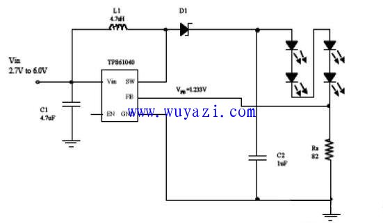
The boost converter in the standard boost converter diagram that drives the white LED is configured as a current source that can drive 4 white LEDs. The device regulates the voltage across the sense resistor Rs to 1.233V to obtain a defined LED current. 
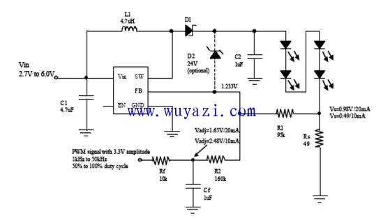
The boost converter used in this configuration will have a voltage drop across the 1.233V current sense resistor, and the power dissipation of the sense resistor will reduce the efficiency of the solution. Therefore, it is necessary to reduce the voltage drop that detects and regulates the LED current. In addition, for many applications, the possibility of adjusting the LED current and LED brightness is also necessary. The circuit in Figure 2 implements these two requirements. 
Figure 2 Improves Efficiency by Reducing Current Sensing Voltage In Figure 2, an optional Zener diode is added to the circuit to clamp the output voltage to prevent an LED from disconnecting or high impedance. A PWM signal with a 3.3V amplitude is applied to the converter's feedback circuit, while a low-pass filter Rf and Cf is used to filter the DC portion of the PWM signal and establish an analog voltage (Vadj) at R2. By changing the duty cycle of the applied PWM signal, the analog voltage is raised or lowered to adjust the feedback voltage of the converter, which increases or decreases the converter's LED current. By applying an analog voltage above R2 to the converter feedback voltage (1.233V), a lower induced voltage can be achieved across the sense resistor. For a 20mA LED current, the induced voltage drops from 1.233V to 0.98V (or even drops to 0.49V for a 10mA LED current).
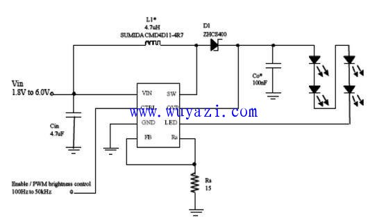
When using a PWM signal with a 3.3V amplitude, the duty cycle that controls the LED brightness must be adjusted from 50% to 100% to get an analog voltage that is typically above the 1.233V feedback voltage. At 50% duty cycle, the analog voltage will be 1.65V, resulting in a 20mA, 0.98V induced voltage. Limiting the duty cycle range between 70% and 100% further reduces the induced voltage. Special LED drivers reduce the number of external components. Figure 3 shows a device that integrates the features described above. The LED current can be controlled by applying a PWM signal directly to the CTRL pin. 
Figure 3 White LED constant current driver IC
Controlling EMI Since both solutions are switching converters running at up to 1MHz switching frequency and can rise and fall quickly, no matter which solution is used (charge pump or boost converter) Special care must be taken. If you are using a charge pump solution, you don't need to use an inductor, so there is no problem with the EMI caused by the magnetic field. However, the flying capacitor of the charge pump solution is continuously charged and discharged by turning the switch on and off at high frequencies. This will cause current spikes and very fast rises and interfere with other circuits. Therefore, the flying capacitor should be as close as possible to the IC connection and the traces should be very short to minimize EMI emissions. A low ESR input capacitor must be used to minimize high current peaks (especially peak currents present at the input).
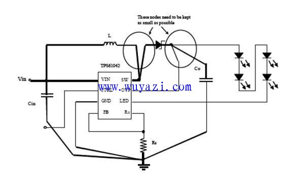
If you are using a boost converter, the shielded inductor will have a more limited magnetic field for better EMI performance. The converter's switching frequency should be chosen to minimize all interference to the wireless portion of the system. The PCB layout will have a major impact on EMI, especially keeping the traces carrying the switch or AC current as small as possible to minimize EMI emissions, as shown in Figure 4. 
Figure 4 Nodes and traces carrying switch currents should be kept to a minimum. Thick traces should be routed first, and a star ground or ground plane must be used to minimize noise. The input and output capacitors should be low ESR ceramic capacitors to minimize input and output voltage ripple. In most applications, boost converters show higher efficiency than charge pumps. Using a boost converter with the same inductor size as the 1210 case size reduces the overall solution size of the charge pump. At least the efficiency needs to be evaluated based on the size of the overall solution. In terms of EMI performance, the design of the boost converter also needs to consider more factors and understanding of more relevant knowledge.
In summary, for many systems, especially when the device has a flexible conversion gain from 1.0 to 1.5, the charge pump solution will be a good solution. Such a solution would achieve excellent efficiency when a conversion gain of 1.0 to 1.5 occurs slightly above the LED forward voltage. When selecting a boost converter or charge pump solution for each application, the key requirements of the portable system need to be fully considered. If efficiency is a key requirement, the boost converter will be a more suitable solution.
Type2 To Type2 EV Charging Cable
Type2 To Type2 Ev Charging Cable,Ev Charging Cable Type 2,Ev Cables,Car Charging Cable
Yangzhou JERI New Energy Co., Ltd. , https://www.jrevcharging.com