
introduction
It is estimated that many novice engineers have found that when the switching frequency of the power supply is increased, the transformer core is less likely to be saturated, or the power of the same power can be made with less magnetic force, even if the switching frequency is not wanted. The limit is increased to reduce the size of the transformer without limitation.
But in fact, the frequency of the general switching power supply is not particularly high, and it is impossible to increase the frequency indefinitely. What are the reasons? Please see below!
Problems such as device limitations, loss, EMI, and difficulty in PCB layout are all factors that limit the infinite increase in switching frequency. Let's expand it a bit!
1, device limitationsFor a switch tube, in practical applications, it is not turned on for a drive, and the drive is turned off. It has turn-on delay time ( t d(on)), rise time ( t r), turn-off delay time ( t d(off)), fall time t f, and the corresponding waveform is as follows:
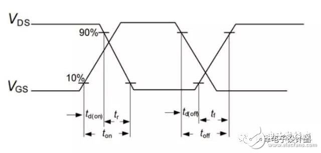
Generally speaking, the opening and closing of the switch tube is not completed instantaneously. It takes a certain time, and the switching time of the switch tube itself limits the increase of the switching frequency.
For example, the author used a 600V coolmos on a 3kW inverter for delta. See how these specific switching times are.
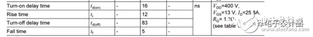
Then for this mos tube, its limit switching frequency (in this limit case, the mos tube is turned off just off) fs=1/(16+12+83+5)ns=8.6MHz, of course, In practical applications, since the duty cycle is adjusted, it is impossible to turn off the switch when it is turned on, so the actual limit frequency is much lower than 8.6 MHz, so the switching speed of the device itself is a factor limiting the switching frequency.
2, switching lossOf course, with the advancement of devices, the speed of the switch is getting faster and faster, especially in low-voltage and low-power applications. If only the switching speed of the device itself is considered, the switching frequency can be run very high, but there is no limit. Above the switching loss.
FigureThe corresponding waveform diagram when the switch tube is actually turned on is given below.
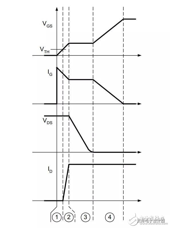
It can be seen that each time the switch is turned on, the voltage of the switch DS (Vds) and the current flowing through the switch (Id) will overlap, resulting in turn-on loss, as well as turn-off. Assume that the energy loss per switch once per switch is fixed, denoted as Esw, then the switch loss power of the switch is Psw=Esw*fs. Obviously, the higher the switching frequency, the greater the switching loss. The switching loss at 5M switching frequency is 10 times larger than that of 500K, which is obviously unacceptable for switching power supplies that emphasize efficiency. Therefore, switching loss is the second factor limiting the switching frequency.
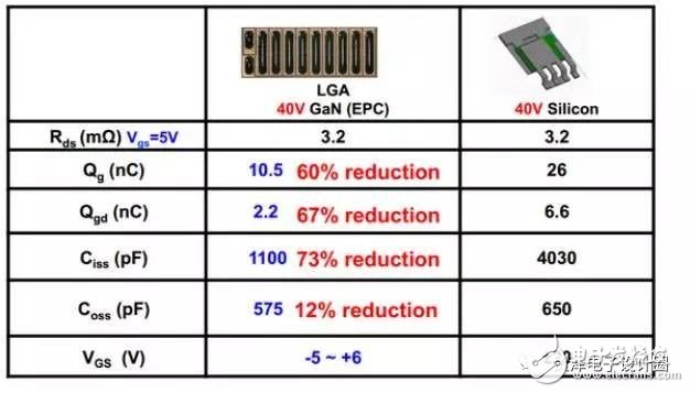
Switching losses are indeed one of the limiting factors, but the introduction of GaN devices has made switch losses acceptable in the 1-3Mhz range.
In the following comparison of a low-voltage gallium nitride and silicon device, it can be seen that, in general, the drive loss will also become small.
It is also important that the wide junction band semiconductor has a high junction temperature. In the current process, the junction temperature of the Sic can operate up to 200° and the gallium nitride can operate up to 150°. For silicon devices, I think that up to 100° is a must. The high junction temperature means that the surface area of ​​the heat sink that needs to be designed for a wide bandgap semiconductor is much smaller under the same loss, and the loss of the wide bandgap semiconductor itself is small.
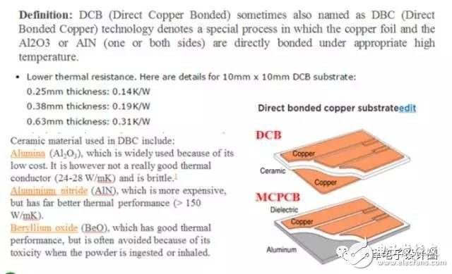
It is the improvement of the switching frequency. It is often only possible to use QFN or other surface mount devices to reduce the parasitic parameters of the package. This brings great challenges to the heat dissipation system. The original To package can be equipped with a heat sink to reduce the thermal resistance to air convection. And now it won't work. So if you want to work at high frequencies, the first problem is to solve the heat dissipation and export the high switching losses, especially at the kW level. The heat dissipation system is very important. Nowadays, the means of solving this problem in the academic circle tends to make the device into a separate package. Using a technology called DCB, the heat dissipation is performed by the ceramic substrate. The thermal resistance of the device from the upper surface to the lower surface of the ceramic is 0.4 ° C / W (some people Metal core PCB is also used, but with an insulating layer, the thermal resistance is generally 4 ° C / W), and FR4 is 20 ° C / W.
Semiconductors are constantly evolving, switching losses are also dropping significantly, and packaging is getting smaller and smaller. Now, what we have to do is how to dissipate that heat from such a small surface mount package.
3, magnetic component lossSkin effect and proximity effect of the winding. When the transformer is operated at high frequencies, the effect is more serious. It will cause a large winding eddy current loss, of course, the switching frequency will increase, and the number of turns of the winding will decrease. The corresponding winding AC impedance becomes larger, but the winding length is reduced. The problem does not seem to be very large. For resonant half-bridge applications, we often choose a frequency of 200KHZ. Such a volume and wear of the magnetic element is a relatively suitable range.
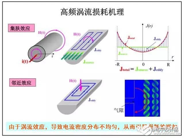
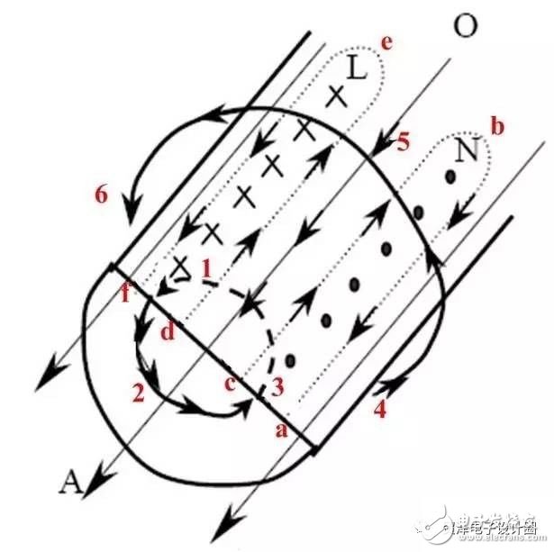
The iron loss of the transformer is mainly caused by the eddy current loss of the transformer. As shown in the figure below, when the high-frequency current is applied to the coil, a changing magnetic field is generated in the conductor and outside the conductor perpendicular to the current direction (1→2→3 and 4→ in the figure) 5→6). According to the law of electromagnetic induction, a changing magnetic field generates an induced electromotive force inside the conductor, and this electromotive force generates eddy currents in the entire length direction (L side and N side) of the conductor (a→b→c→a and d→e→f→d). Then, the main current and the eddy current are strengthened on the surface of the conductor, and the current tends to the surface. Then, the effective AC cross-sectional area of ​​the wire is reduced, resulting in an increase in the AC resistance (eddy current loss coefficient) of the conductor and an increase in loss.
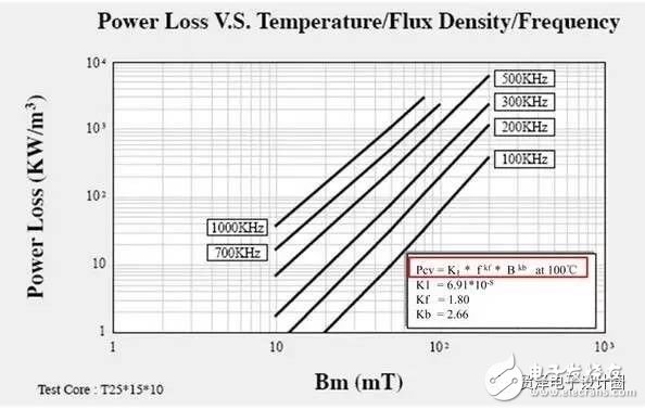
As shown in the figure below, the transformer iron loss is proportional to the kf power of the switching frequency, and is related to the magnetic temperature limitation. Therefore, as the switching frequency increases, the high-frequency current flows in the coil to generate a severe high-frequency effect. The conversion efficiency of the transformer is lowered, and the temperature of the transformer is increased, thereby limiting the switching frequency.
The subject mentioned soft switching, yes, the soft switch is indeed a powerful means of solving switching losses. On the various papers that study soft switches, there are countless kinds of dazzling soft switching schemes. It seems that soft switching can solve all problems. However, the actual engineering application is different from the theoretical analysis. The actual engineering pursues low cost, high efficiency, high reliability, and those soft switching schemes that need to add a bunch of auxiliary circuits or have very precise control are actually not very practical in actual engineering. It is optimistic, so even now, the most commonly used softswitch topology in the industry is only the phase shift full bridge and some resonant topologies (such as LLC). As for the flyback mentioned by the subject, yes, I also heard There is a quasi-resonant flyback (but not studied), but even if there is a similar solution, for the real engineering application, the subject needs to consider several issues mentioned above.
Ps, for low-power high-frequency power supply, class E is very hot now, I think the reason for it is that the circuit is simple, so it can be accepted by the industry, the subject is interested to study.
5, a series of problems caused by high frequencyAssuming that the above series of problems have been solved, the real high frequency also needs to solve a series of engineering problems. For example, at high frequencies, the parasitic parameters of the circuit often seriously affect the performance of the power supply (such as the original secondary side of the transformer). Parasitic capacitance, transformer leakage inductance, parasitic inductance and parasitic capacitance between PCB wiring, etc.), causing a series of voltage and current waveform oscillations and EMI problems, how to eliminate the effects of parasitic parameters, and even further, how to use parasitic parameters Circuit services are issues to be studied.
Ps, for the practical engineering application of high-frequency applications, there is also a very important piece of high-frequency drive circuit design.
Of course, with the rise of new devices (SiC, GaN), research on high-frequency switching power supplies is on the rise, and the high frequency of switching power supplies must be a trend, and it is expected to bring another revolution to power electronics. let us wait and see.
6, EMI and interference, PCB layout is more difficultBefore I came into contact with EMI, many old engineers used their rich experience in EMI debugging to despise our rookies. I always thought that EMI was a mystery, and many people were scared by EMI. I want to say that EMI is really difficult to understand. It is difficult to have accurate paper design, but through research we can still know the general trend to guide the design, rather than some engineering and error process. I will first conclude that EMI does not have a linear relationship with the switching frequency. At some switching frequencies, the EMI filter has a higher turning frequency, but in terms of overall trend, the higher the switching frequency, the smaller the EMI volume!
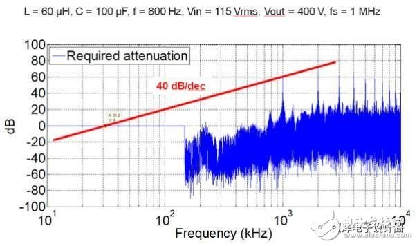
I know that a lot of people may start to spray me, how is it possible, di/dt and dv/dt are big, how can the EMI filter volume be small? I want to say that there is no difference between the common mode and the differential mode filter. At the same cutoff frequency, the attenuation of the high frequency is greater! Even if you have a higher common mode noise at high frequencies, you remember that the attenuation of the LC filter is greater at this frequency. Think about the amplitude-frequency curve. To illustrate this conclusion, I give some quantitative analysis results. These EMI analyses are based on AC/DC three-phase rectification with a topology rectified by Vienna. I gave the common mode noise of 1Mhz and 500Khz respectively. It can be seen that the 500khz common mode filter requires a cutoff frequency of 19.2kHz and 1MHz of 31.2kHz.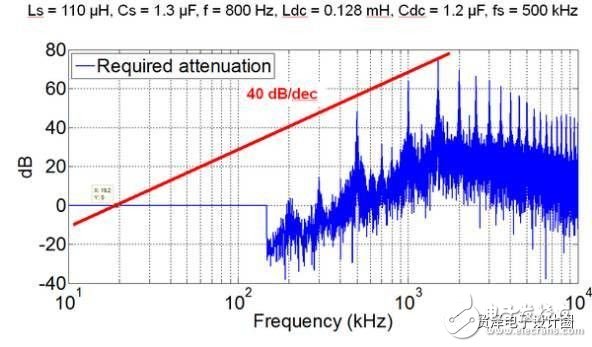
Assuming that the power device loss described above is solved, the real high frequency also needs to solve a series of engineering problems, because at high frequencies, the inductor is not the inductor we are familiar with, the capacitor is not the capacitor we know, all the parasitic parameters. Corresponding parasitic effects will be generated, which will seriously affect the performance of the power supply, such as the parasitic capacitance of the transformer's primary side, the leakage inductance of the transformer, the parasitic inductance and parasitic capacitance between the PCB wiring, which will cause a series of voltage and current waveform oscillations and EMI problems. The voltage stress of the switch tube is also a test.
7, summaryNot the higher the switching frequency, the higher the power density. At this stage, the real obstacle to power density improvement is the heat dissipation system and electromagnetic design (including EMI filters and transformers) and power integration technology.
Careful selection of the switching frequency, the switching frequency will greatly affect the power density of the entire variator, and the optimal switching frequency varies for different devices, topologies.
High frequencies do generate a lot of interference problems that are difficult to solve. It is often necessary to find the interference loop and then take some measures.
In order to continue to maintain the growth trend of power electronic converter power density, high frequency is definitely a trend. Only the power electronics technology for high-frequency design is immature, the related supporting chips have not met the requirements, and some high-frequency electromagnetic design theories are imperfect and accurate. The use of finite element software analysis will greatly increase the development cycle.
To improve the power density of switching power supply products, the first consideration is to increase the switching frequency, which can effectively reduce the volume of transformers, filter inductors and capacitors, but it is faced with losses caused by switching frequency, which makes the design of temperature rise heat dissipation difficult. The increase in frequency will also lead to a series of engineering problems such as driving and EMI.
KNB6-40 Miniature Circuit Breaker
KNB6-40 Mini Circuit breakers, also named as the air switch which have a short for arc extinguishing device. It is a switch role, and also is a automatic protection of low-voltage electrical distribution. Its role is equivalent to the combination of switch. Fuse. Thermal Relay and other electrical components. It mainly used for short circuit and overload protection. Generally, According to the poles, mini Circuit breaker can be divided into 1P , 1P+N , 2P, 3P and 4P.
KNB6-40 Miniature Circuit Breaker,Electronics Miniature Circuits Breaker,Automatic Miniature Circuit Breaker,Mini Circuit Breaker
Wenzhou Korlen Electric Appliances Co., Ltd. , https://www.korlenelectric.com