First acquainted with FPGA CLB LUT to realize RAM
I. Overview
In the article "First Understanding FPGA CLB LUT Realization Logic Function", we have talked about the principle of LUT. When implementing a logic function, it is equivalent to a ROM to pre-store the result, and then use the input signal as an address to address the pre-stored result . Therefore, RAM can be realized by adding several ports with the same LUT. The LUT in SLICEM can be used to implement RAM resources.
2. Principle Introduction
Compared with the LUT in SLICEL, the LUT in SLICEM has more ports of DI2, WA[6:1], CLK, and WE. When used as RAM, DI1 and DI2 are write data input ports, and O5 and O6 are also data output ports, supporting one-time two-bit or single-bit read and write. A[6:1] is the read address, WA[6:1] is the write address, WE is used for writing, and CLK is the clock port.
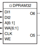
It can be seen from this that a LUT has 2^6=64bit storage space.
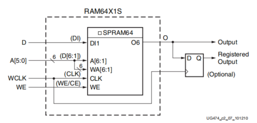
Therefore, a LUT can be used as a 64x1bits RAM (the memory size is 64bit, 1bit read and write), and the address is 6 bits. When the read and write addresses share one port, it is a single-port RAM, and when it is not shared, it is a dual-port RAM (WA and A of the first LUT in SLICEM are connected together, so the first LUT cannot be a dual-port RAM). The output data can be beaten by the Register resource in SLICEM to improve the timing characteristics (you can set it yourself in the tool).
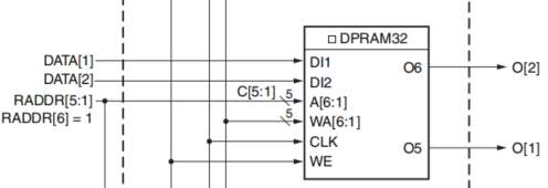
Or as a 32x2bits RAM (2bit read and write), the address is 5 bits, and A[6] is pulled high. The output is O5, O6.
3. Expansion and improvement
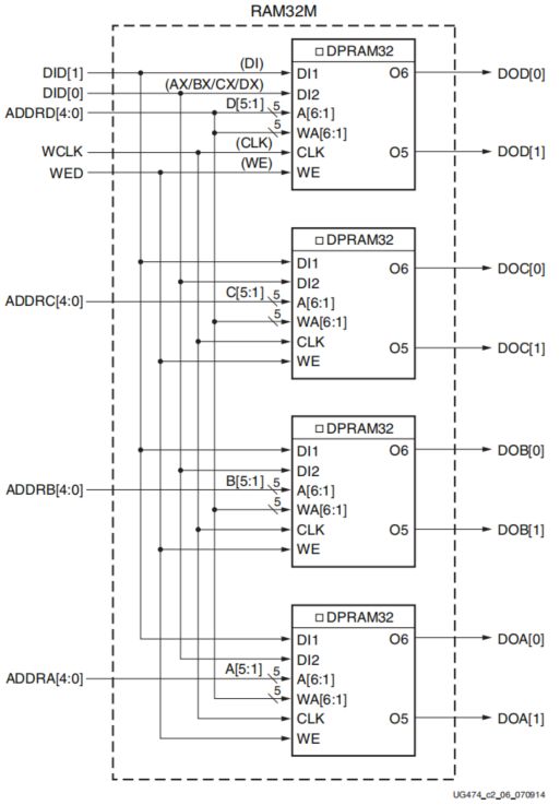
There are 4 LUTs in a SLICEM, and they can be combined to get various sizes of RAM. The first is the four-port 32x2bits RAM, which supports one-time reading and writing of 2bits. The principle is as shown in the figure below. The write data ports DI1, DI2, write enable WE, and write address WA of the four LUTs are shared, which is called write control signal sharing. The read address A is controlled separately.
As shown in the figure below, 4 LUTs form a 32x6bits RAM, which supports 6bits read and write operations. When reading and writing share an address, it is a single-port RAM, and when reading and writing do not share an address, it is a dual-port RAM. It can be seen that the first LUT is actually useless, because the A and WA of the first LUT are connected together and cannot be changed, so dual ports cannot be implemented. Its realization principle is parallel 2bit reading and writing of 3 LUTs.
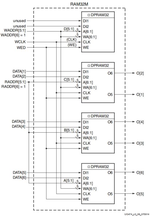
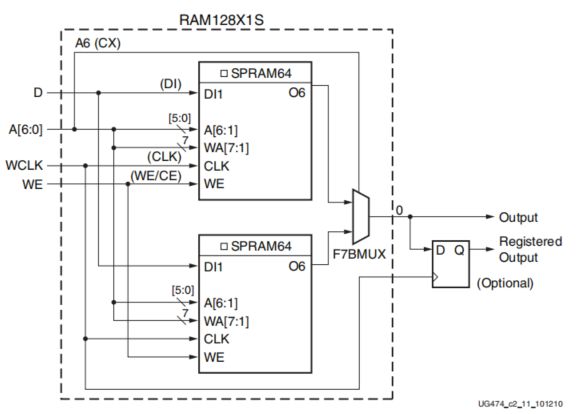
Of course, if you use your own brains and think about it, you will know what other types of RAM can be formed. Here we will give another example to achieve 128x1bits RAM with the help of selectors.
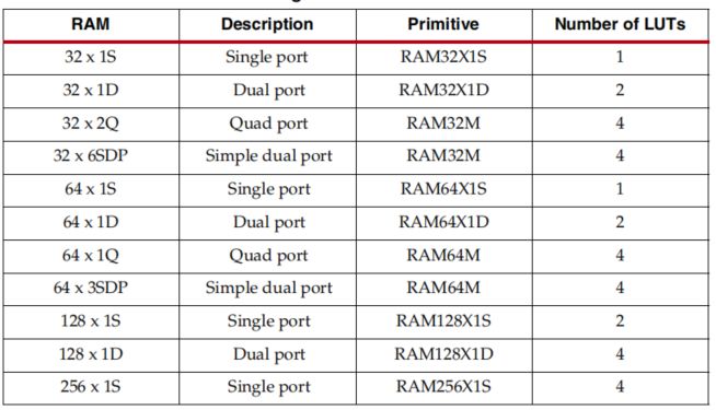
Similarly, a 256x1bit RAM can be formed in a SLICEM with the help of selectors. I won't go into details here, you can think about it yourself. In short, there are several types of RAM that can be implemented in a SLICEM as shown in the following table.
Multiple SLICEM resources can be combined to form more types of RAM.
Insulation Paper Dmd,Insulfrax Paper,Silver Paper Insulation,Battery Insulation Paper
Longkou Libo Insulating Material Co.,Ltd. , https://www.sdliboinsulation.com