As a traditional voice pickup tool, a single isolated microphone has shortcomings in noise processing, sound source localization and tracking, voice extraction and separation, which seriously affects the quality of voice communication. If multiple microphones are used to form an array, adding a spatial domain based on the time-frequency domain and real-time processing signals from different directions in the space can make up for the above shortcomings. In the existing microphone array acquisition and processing systems, 4 microphone arrays are mostly used. Although such systems can solve the problems of speech enhancement, noise suppression, sound source localization and echo cancellation to some extent, due to the number of 4 microphones. Less, can only form a word line array, cross array and other specific array shapes, the direction and distance of the three-dimensional space is judged to have a large error. The designed 16-channel microphone acquisition system can form a microphone array, which makes up for the above shortcomings and better solves the problem of position determination of three-dimensional space signals.
First, the hardware system design
The hardware system mainly includes an array of 16 microphones, an A/D sampling module, a DSP data processing module, and a PC, as shown in FIG.
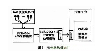
1.1 Microphone array In this system, the microphone array uses Prestige's MPA416 microphone. The MPA416 microphone has a sensitivity of 50 mV/Pa; it has a low noise floor; the frequency response range is 20 Hz to 20 kHz; when it is used in an array, the phase difference of the MPA416 can be controlled from 3° to 5°, which can satisfy the system pair. Precision and stability requirements.
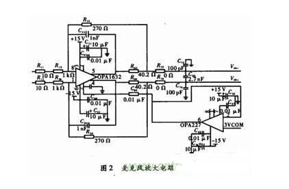
1.2 A/D sampling module The A/D sampling module consists of four PCM4204s and its peripheral circuits. The PCM4204 has four simultaneous sampling channels built in to support the audio serial port and DSD data port. In the audio serial port mode, the 24-bit linear PCM code is output. It has both active and passive modes of operation. It supports left and right alignment, I2S and TDM data formats. The dynamic range is 118 dB and the maximum sampling frequency is 216 kHz. The system selects one PCM4204 to adopt active working mode, and the other three PCM4204 adopt passive working mode. The externally acquired analog sound signal is converted into a 24-bit I2S format digital signal through the audio serial port. Since the output signal of the front-end microphone array is not a differential signal, and the PCM4204 requires the input signal to be a differential signal, and the input differential signal amplitude is between -0.3 and -0.3+VccV, there should be a buffer at the front end of each signal. A circuit that converts the received microphone signal into a differential signal and adjusts the amplitude. The snubber circuit is mainly composed of OPA1632 and OPA22. The OPA1632 and OPA227 are high-precision, audio differential amplifiers. The snubber circuit is shown in Figure 2.
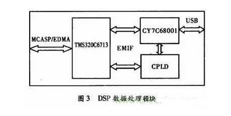
1.3 DSP data processing module design data processing module select TI company floating-point DSP chip TMS320C6713 as the module core. The TMS320C6713 is a high-performance 32-bit floating-point DSP for professional audio signal processing with a frequency range of up to 300 MHz and processing speeds of up to 2 400 MIPS/1 800 MFLOPS. It has an improved Harvard architecture internally; it has 256 kB of on-chip memory; rich peripherals include two multi-channel buffered serial ports (McBSP), two multi-channel audio serial ports (McASP), SPI and I2C, etc.; Memory Access (EDMA) controller that controls 16 independent channels for data transfer without CPU intervention; 32-bit External Memory Interface (EMIF) for seamless connection to SRAM, ERPOM, Flash, SBSRAM, and SDRAM. The block diagram of the DSP data processing module is shown in Figure 3. Among them, TMS320C6713 is connected to the front-end A/D sampling module through McASP, and uses EDMA data transmission speed, large transmission capacity, and does not occupy the characteristics of CPU clock cycle, and the collected data is transferred to the on-chip storage space of TMS320C6713. The TMS320C6713 external CPLD controls the EMIF interface. By controlling the CE3 space on the EMIF interface, the USB chip CY7C680 01 is controlled to complete the USB data transmission between the TMS320C6713 and the PC platform.
1.4 A/D sampling module and DSP data processing module interface design Four PCM4204 chips are connected with McASP1 of TMS320C6713, and the connection diagram is shown in Figure 4.
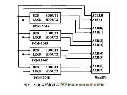
In Figure 4, the PCM4204 A uses the active mode of operation, and the PCM4204B, PCM4204C, and PCM4204D use the passive mode of operation. The system uses the I2S data format. The SDOUT1 of the PCM4204A outputs 1 and 2 channels of data, the SDOUT2 outputs 3 and 4 channels of data, the PCM4204B's SDOUT1 outputs 5 and 6 channels of data, and the SDOUT2 outputs of 7 and 8 Channel data; PCM4204C's SDOUT1 outputs 9 and 10 channels of data, SDOUT2 outputs 11 and 12 channels of data; PCM4204D's SDOUT1 outputs 13 and 14 channels of data, and SDOUT2 outputs of 15 and 16 channels data.
The PCM4204 is set by configuring the chip pins S/M, FMT2, FMT1, FMT0, FS2, FS1, and FS0.
1.5 DSP data processing module USB interface design TMS320C6713 can extend the USB2.0 interface through the EMIF CE3 storage space. Therefore, before reading/writing access to the external expansion USB, CE3 space memory needs to be configured through the EMIF CE3 control register CE3C-TL. Interface type, memory width, and read and write timing. CY7C68001 uses parallel asynchronous memory interface to connect with TMS320C6713 through programmable logic chip CPLD. The block diagram is shown in Figure 5.
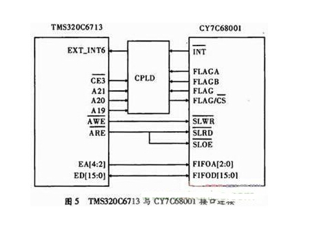
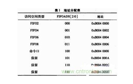
And 4 status signals. The interrupt signal uses the external interrupt EXT_INT6 of the TMS320C6713. The TMS320C6713 uses CY7C68001 as a slave device. In this mode, the DSP can read/write the FIFO inside the CY7C68001 like a normal/read FIFO. When the PC host issues a command, the interrupt trigger signal is also supplied to the EXT_INT6 of the DSP by the pin of CY7C68001. After its rising edge is detected, the DSP enters the corresponding interrupt service routine and begins processing USB transfers. The DSP selects the FIFO or command port of the CY7C68001 by connecting FIFOA[2:0] through EA[4:2]. The read/write data is connected to FIFO[15:0] via ED[15:0]. The selection and address assignment of FIFO and command port are shown in Table 1.
It has been verified by experiments that the USB asynchronous transmission rate can reach 3 Mbit?s-1, which satisfies the system requirements.
1.6 The PC data processing module of the PC platform is connected to the PC through the USB interface, and the data collected by the front end is transmitted to the PC through the CY7C68001 chip, which facilitates further processing of the data.
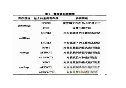
Second, the program design 2.1 McASP interface program design defines four register groups: global register group globalRegs, send register group xmtRegs, receive register group mvRegs and serializer control register group srctlRegs. Through these four register sets, registers such as PFUNC, PDIR, SRCTL, RFMT, AFSRCTL, ACLKRCTL and AHCLKRCTL of McASP1 are set. The main registers included in each register bank are shown in Table 2.
According to the I2S data format of the PCM4204, the width of the received frame synchronization signal is set to 32 bits, the reception delay is set to 1 delay, and AXR[0] to AXR[7] are set to the reception mode.
2.2 EDMA transfer program is designed to ensure data integrity. Ping-Pong mode is used to configure EDMA transfer. Ping cache is stored as shown in Table 3. Pong cache is the same as Ping cache.
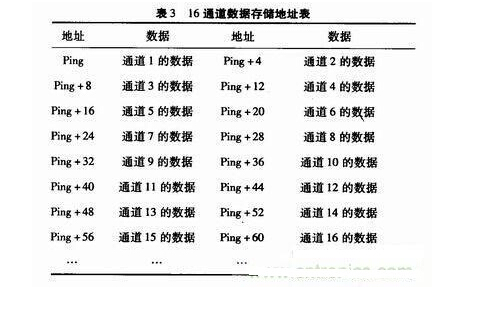
According to the Ping and Pong cache data formats, the EDMA reception is configured, that is, the EDMA opt, src, cnt, dst, idx, and rld registers are respectively set. The data length is set to 32 bit through the opt register, the source data and the destination data are in one-dimensional mode, the source address is fixed, the destination address is indexed, and frame synchronization is enabled. The source and destination addresses are written to the src, dst registers, respectively. The cnt register is mainly used to configure the frame count and unit count. Since the data format of I2S is adopted, one frame of data contains only two unit data. By configuring the idex and rld registers, the destination data can be stored in the set index.
2.3 DSP-side OSB interface program design First, the external interrupt is enabled and the USB register is initialized by calling the user's initialization function. After that, the program completes the data transmission between the DSP and the PC through the data transfer function.
The USB initialization program is configured as follows:
(1) Enable external interrupt 6 (EXT_INT6).
(2) Load the USB description table and perform bootstrap detection. If the bootstrap is unsuccessful, restart the bootstrap until endpoint 0 receives the setup packet.
(3) Configure USB as asynchronous FIFO (Asynchronous SlaveFIFO) mode, using internal 48 MHz clock source.
(4) Read the FNADDR register to determine the USB operating status.
(5) According to the USB working state, configure EP2, EP4, EP6, EP8, and set the Byte length of one transmission. Set EP2, EP4 to BULK OUT, EP6 and EP8 to BULK IN, and the buffer size is 2 × 512 Byte.
During the data transmission process, the PC sends a read data command to the DSP through EP2. After receiving the read command through the external interrupt, the DSP uses EP6 to send the collected data. In the sound data acquisition system, each microphone is sampled at 24 kHz for 24 bits and stored in ping-pong mode. In the transmission process, it is also necessary to judge, when the collected data is stored in the ping cache, the data in the pong cache is sent, and when the collected data is stored in the pong cache, the ping cached data is sent. Since the TMS320C6713 can expand the USB2.0 interface through the EMIF CE3 memory space, configure the CE3 register of the EMIF interface, set the USB interface to the 16-bit asynchronous storage interface, and set the read/write setup time (Setup). Strobe, hold time, to meet the read/write timing requirements of CY7C68001.
2.4 PC platform application program design PC-side interface program is written in VC++6.0, first call OpenDriver () to open the USB interface device, obtain the device handle hDevice, then call the Sx2SendVendorReq () function to issue commands to the peripherals, read the USB configuration Finally, Sx2BulkdataTrans() is called for data transfer, and the received data is stored in a text file by calling the CFile class. The program uses multi-threading technology, which allows the application to process USB data transfers in the background, and the application foreground can perform other operations.
100W Portable Solar Panels,Mini Solar Panel,Watt Solar Panel,Portable Folding Solar Panel
Guangzhou Fengjiu New Energy Technology Co.,Ltd , https://www.flashfishbatteries.com