/////////////////////////////////////////////////// /////////////////////////
SiP, system in package; This is not a brand-new technology, in fact has appeared for a long time, but recently with the rise of internet of things and wearable device, we see more and more words of SiP.
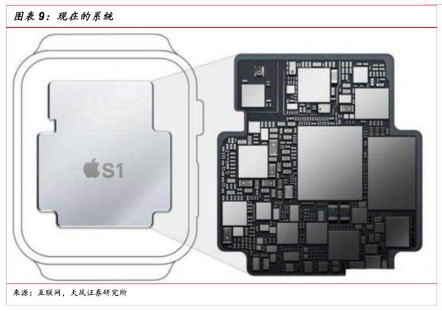
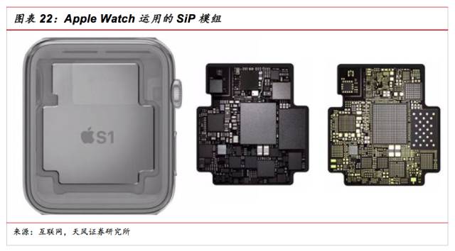
Apple watch is a typical example. Apple encapsulates all APs, modems, TRCVs, and RFFEs in a single SiP product. This is an amazing new approach. From the RF point of view, engineers are coupling, coexistence, and interference. How much effort has been made is self-evident;
In the field of C-IoT Internet of Things, we also see more and more chip suppliers trying out SiP solutions. Today we have seen three SiP products on the market, namely Nordic modem + Qorvo RFFE. Sequans modem + Skyworks RFFE, Altair modem+ Murata RFFE.
These brand-new products, which have great advantages in terms of performance and size, can not help but be more curious about SiP technology. What are the characteristics of SiP and the difference between it and SOC?
We can learn reference together through this article.
1 Beyond the Moore Road - Introduction to SiP
According to the definition of the International Semiconductor Routes Organization (ITRS): SiP to preferentially assemble a plurality of active electronic components with different functions and optional passive components, as well as other devices such as MEMS or optical devices, to achieve a certain function of the single Standard packages form a system or subsystem.
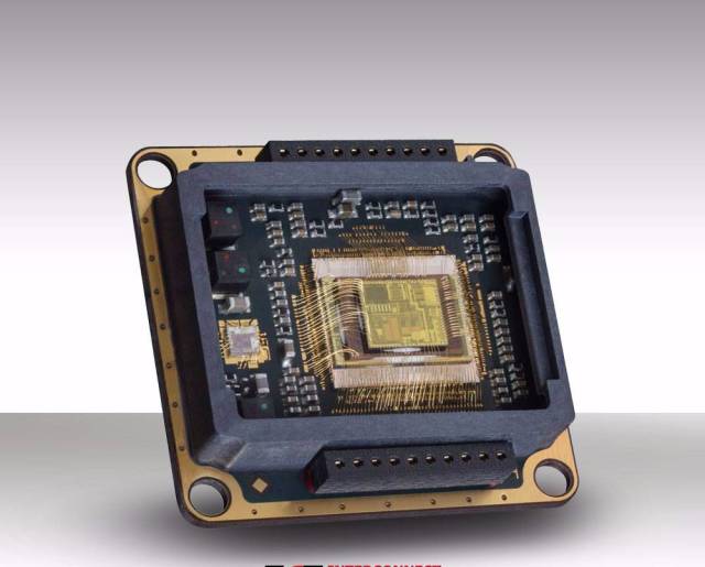
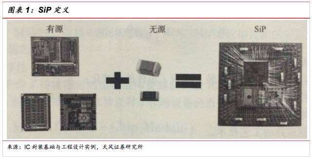
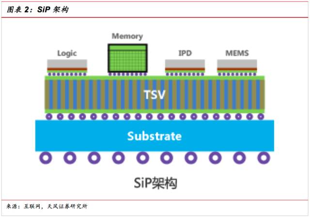
From an architectural perspective, SiP integrates a variety of functional chips, including processor, memory, and other functional chips in a single package, to achieve a basic and complete function. Corresponds to the SOC (system on chip). The difference is that the system-level package is a side-by-side or superimposed package using different chips, and the SOC is a highly integrated chip product.
1.1. More Moore VS More than Moore - Comparison of SoC and SiP
SiP is an important implementation path beyond Moore's Law. Well-known Moore's Law has developed to the present stage. Where do we go from here? There are two paths in the industry: First, continue to develop in accordance with Moore's Law. Products that follow this path include CPU, memory, and logic devices. These products account for 50% of the market. The other is more than Moore's Law's more than Moore line, chip development from the blind pursuit of power consumption and performance improvement, to more pragmatic to meet market demand. The products in this area include analog/RF devices, passive devices, power management devices, etc., accounting for about 50% of the remaining market.
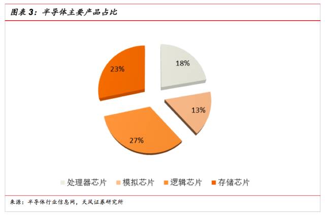
For these two paths, two products were born: SoC and SiP. SoC is the product of Moore's Law continuing to go down, and SiP is an important way to achieve beyond the law of Moore. Both are products that achieve miniaturization and miniaturization at the chip level.
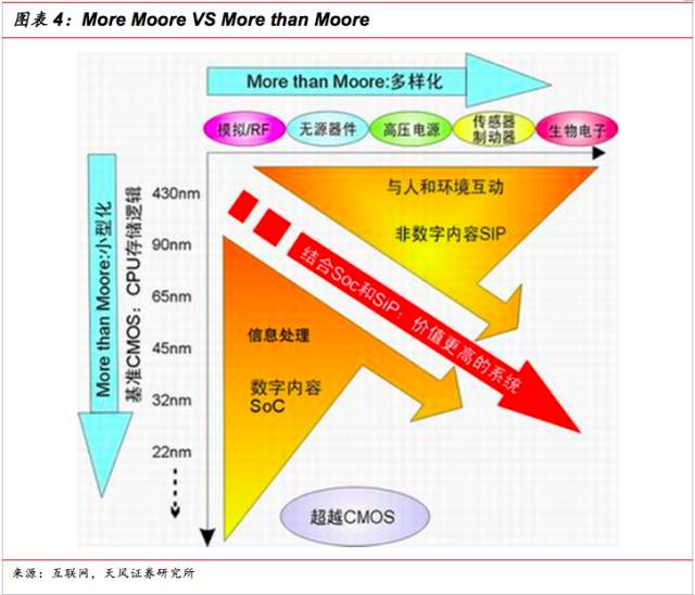
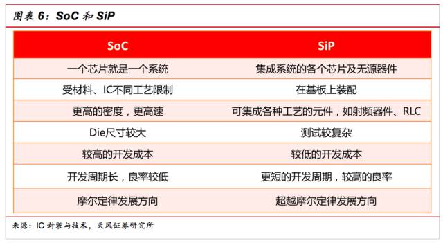
SoC and SIP are very similar, both of which integrate a system containing logical components, memory components, and even passive components into one unit. SoC is from the design point of view, is to highly integrate the components required by the system into a single chip. SiP is based on the package's standpoint, where different chips are stacked side-by-side or stacked. Multiple active electronic components with different functions and optional passive components, as well as other devices such as MEMS or optics, are preferentially assembled together. A single standard package that achieves a certain function.
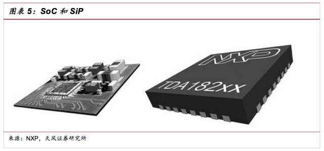
In terms of integration, under normal circumstances, the SoC only integrates logic systems such as APs, and SiP integrates AP+mobile DDR, to a certain extent SIP=SoC+DDR, with increasing integration in the future, Emmc is also very likely to integrate into SiP.
From the point of view of package development, SoC has been established as the key and development direction of electronic product design in the future due to the demand for electronic products in terms of volume, processing speed or electrical characteristics. However, with the increasing production costs of SoC in recent years, technical obstacles frequently encountered, resulting in the development of SoC bottlenecks, and thus making the development of SiP more and more attention by the industry.
1.2. SiP - The Inevitable Choice to Overtake Moore's Law
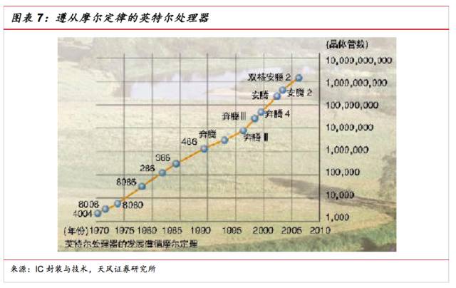
Moore's Law ensures the continuous improvement of the performance of the chip. As we all know, Moore's Law is the "Bible" for the development of the semiconductor industry. On silicon-based semiconductors, the feature size of transistors is reduced by half every 18 months, and the performance is doubled. At the same time as the performance increases, the cost is reduced. This allows semiconductor manufacturers to have sufficient incentive to achieve the reduction of semiconductor feature sizes. Among them, the processor chip and the memory chip are the two types of chips that most comply with Moore's Law. Taking Intel as an example, each generation of products perfectly follows Moore's Law. On the chip level, Moore's Law promotes the continuous advancement of performance.
The PCB board does not comply with Moore's Law and is the bottleneck of the overall system performance improvement. Corresponding to the shrinking chip size, PCB boards have not changed much in these years. For example, the standard minimum line width of a PCB board is 3 mils (approximately 75 um) from ten years ago, and it is still 3 mils today, with little progress. After all, PCB does not follow Moore's Law. Because of the limitations of the PCB, the performance of the entire system has encountered a bottleneck. For example, because the PCB line width has not changed, the connection density between the processor and the memory remains unchanged. In other words, the number of wires between the processor and the memory does not change significantly in the case where the size of the processor and the memory package do not change. The memory bandwidth is equal to the memory interface bit width multiplied by the memory interface operating frequency. The memory output bit width is equal to the number of connections between the processor and the memory, which has been unchanged by the PCB board technology for a decade. Therefore, if you want to increase the memory bandwidth, you only need to increase the operating frequency of the memory interface. This limits the performance of the entire system.
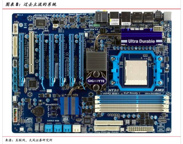
SIP is the solution to the success of the system. A plurality of semiconductor chips and passive devices are packaged in the same chip to form a system-level chip, and no PCB is used as a carrier for connecting the chip connections, and the system performance can be solved due to a congenital deficiency of the PCB itself. A bottleneck problem. Taking processors and memory chips as an example, the density of the internal traces in the system-level package can be much higher than the PCB trace density, thus solving the system bottleneck of PCB lines. For example, because the memory chip and the processor chip can be connected together in a punched manner, no longer limited by the PCB line width, the data bandwidth can be improved in the interface bandwidth.
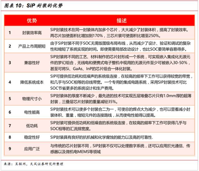
We believe that SiP is not just simply integrating the chips together. SiP also has the advantages of short development cycle, more functions, lower power consumption, better performance, lower cost, smaller size, and lighter weight. It is summarized as follows:
2SiP process analysis
SIP packaging process can be divided into wire bonding package and flip-chip bonding according to the connection between chip and substrate.
2.1. Wire Bonding Packaging Process
The main process of wire bond packaging process is as follows:
Wafer → wafer thinning → wafer cutting → chip bonding → wire bonding → plasma cleaning → liquid sealant potting → assembly solder balls → reflow soldering → surface marking → separation → final inspection → testing → packaging.
Thin wafers
Thinning wafers refers to the use of mechanical or chemical mechanical (CMP) polishing from the back side of wafers to thin the wafers to a level suitable for encapsulation. Due to the increasing size of wafers, in order to increase the mechanical strength of wafers and prevent deformation and cracking during processing, its thickness has been increasing. However, as the system develops in the direction of light weight and thinness, the thickness of the module after the chip is packaged becomes thinner and thinner. Therefore, the thickness of the wafer must be reduced to an acceptable level before packaging to meet the requirements for chip assembly.
Wafer cutting
After the wafer is thinned, it can be diced. The older dicing saws were manually operated, and now the general dicing machines have been fully automated. Regardless of whether it is a partially-divided or fully-divided silicon wafer, a saw blade is currently used because it has a neat edge with few debris and cracks.
Chip bonding
The cut chips are mounted on the center pad of the frame. The size of the pad must match the size of the chip. If the pad size is too large, the lead span will be too large. Due to the stress generated during the transfer process, the lead will bend and the chip will be displaced. The mounting method can be soldered to the substrate with soft solder (referred to as Pb-Sn alloy, especially Sn-containing alloy), Au-Si eutectic alloy, etc. The most common method in plastic packaging is to use polymer adhesive. The adhesive is applied to the metal frame.
Wire bonding
Leads used in plastic packages are mainly gold wire, and their diameter is generally 0.025mm~0.032mm. The length of the lead is usually between 1.5mm and 3mm, and the height of the arc can be 0.75mm higher than the plane where the chip is located.
Bonding technology has hot pressure welding, thermal ultrasonic welding and so on. These technical advantages are that it is easy to form a ball (that is, solder ball technology) and prevent oxidation of the gold wire. In order to reduce the cost, other metal wires such as aluminum, copper, silver, palladium, etc. are also being studied instead of gold wire bonds. The conditions of thermal pressure welding are that the two metal surfaces are in tight contact with each other, and the time, temperature and pressure are controlled so that the two metals are connected. Surface roughness (unevenness), the formation of an oxide layer or chemical contamination, moisture absorption, etc. will affect the bonding effect and reduce the bonding strength. The temperature of thermal welding is between 300°C and 400°C, and the time is generally 40ms (usually, plus the search for the bonding position and other procedures, the bonding speed is second line per second). Ultrasonic welding has the advantage of avoiding high temperatures because it uses ultrasonic vibrations from 20 kHz to 60 kHz to provide the necessary energy for welding, so the welding temperature can be reduced. The simultaneous use of heat and ultrasonic energy for bonding is so-called thermosonic welding. Compared with hot-press welding, the biggest advantage of thermosonic welding is to reduce the bonding temperature from 350°C to 250°C (others think that 100°C~150°C can be used), which can be greatly reduced on the aluminum pad. The possibility of forming an Au-Al intermetallic compound extends the lifetime of the device while reducing the drift of circuit parameters. The improvement in wire bonding is mainly due to the need for thinner and thinner packages, and the thickness of some ultra-thin packages is only about 0.4 mm. Therefore, the loop length is reduced from the general 200 μm to 300 μm to 100 μm to 125 μm, so that the tension of the lead wire is very large and the tension is very tight. In addition, there are usually two ring power/ground lines on the periphery of the lead pad on the substrate. To prevent the gold line from short-circuiting during bonding, the minimum gap must be >625 μm. This requires that the bonding lead must have high linearity. And a good arc.
Plasma cleaning
One of the important effects of cleaning is to improve the adhesion of the film, such as depositing an Au film on a Si substrate, removing surface hydrocarbons and other contaminants by Ar plasma, and significantly improving the adhesion of Au. The surface of the plasma-treated substrate will leave behind a layer of fluoride-containing gray matter that can be removed with a solution. Simultaneous cleaning also helps improve surface adhesion and wetting.
Liquid sealant potting
Place the frame tape that has been mounted on the chip and complete the wire bonding in the mold, heat the pre-molded block of molding material in the preheating furnace (preheating temperature is between 90° C. and 95° C.), and then put it into the transfer. Molding machine in the transfer tank. Under the pressure of the transfer molding piston, the molding compound is extruded into the runner and injected into the mold cavity through the gate (in the whole process, the mold temperature is maintained at about 170°C~175°C). The plastic material rapidly solidifies in the mold, and after a period of pressure keeping, the module reaches a certain hardness, and then ejects the module with the ejector rod, and the molding process is completed. For most molding compounds, after the pressure is maintained in the mold for a few minutes, the hardness of the module is sufficient to allow ejection, but the curing (polymerization) of the polymer is not completed. Since the degree of polymerization of the material (degree of cure) strongly influences the glass transition temperature and the thermal stress of the material, it is very important to promote the stability of the material in order to improve the reliability of the device. The post-curing is to improve the plastic sealing material. The degree of polymerization and the necessary process steps, the general post-curing conditions are 170 °C ~ 175 °C, 2h ~ 4h.
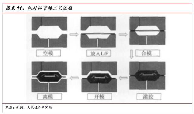
Liquid sealant potting
Currently, there are two ball-planting methods used in the industry: "tin paste" + "tin ball" and "solder paste" + "tin ball." The solder paste + solder ball ball-planting method is the industry-recognized best standard ball-planting method. Balls implanted in this way have good solderability and luster, and solder ball offset phenomenon does not occur during the solder melting process. , easier to control, the specific approach is to first solder paste printed on the BGA pad, and then use a ball machine or screen printing with a certain size of the solder ball, then the role of solder paste is to stick tin The ball, when heated, allows the contact surface of the solder ball to be larger, so that the solder ball is heated faster and more comprehensively, so that the solder ball is soldered to the solder pad better after solder melting, and the possibility of soldering is reduced.
Surface marking
Marking is to print on the top surface of the package module unremovable, handwritten letters and logos, including manufacturer's information, country, device code, etc., mainly for identification and tracking. There are several ways to code, the most common of which is the method of printing, and it includes ink printing and laser printing.
Separation
In order to increase production efficiency and save material, most of the SIP assembly work is done in an array combination. After the molding and testing processes are completed, they are divided into individual devices. Segmentation can be divided into sawing or stamping processes. The sawing process is relatively flexible and does not require much special tools. The stamping process is relatively high in production efficiency and low in cost, but requires special tools.
2.2. Flip Chip Process
The flip-chip welding process compared with the wire bonding process has the following advantages:
(1) Flip-chip welding technology overcomes the problem of the center distance of the wire bond pad;
(2) Provides more convenience to electronic designers in the design of the power/ground distribution of the chip;
(3) By shortening the interconnect length and reducing the RC delay, providing a more complete signal for high-frequency, high-power devices;
(4) Excellent thermal performance, and the radiator can be installed on the back of the chip;
(5) high reliability, due to the role of the filler under the chip, the anti-fatigue life of the package is enhanced;
(6) Easy to repair.
The following is the process flow of flip-chip bonding (the same part of the process as wire bonding is not described separately): wafer → pad redistribution → wafer thinning, bump making → wafer cutting → flip-chip bonding, Fill under → encapsulate → solder balls → reflow → surface marking → separation → final inspection → test → packaging.
Pad redistribution
In order to increase the lead pitch and meet the requirements of the flip chip process, the leads of the chip need to be redistributed.
Making bumps
After the pad redistribution is completed, bumps need to be added on the pads on the chip. The solder bump manufacturing technology may use electroplating, electroless plating, evaporation, ball placement, and solder paste printing. Electroplating is still the most widely used method, followed by solder paste printing.
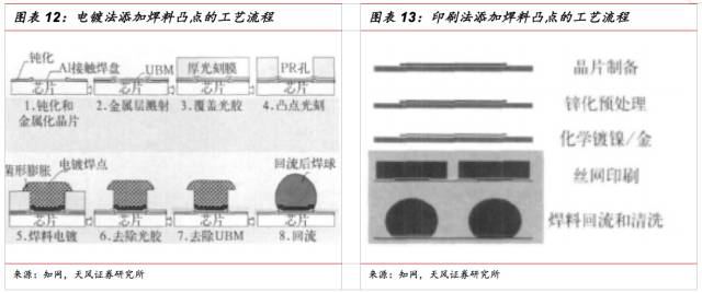
Flip-chip bonding, underfill
After the solder bumps are arranged in a grid array shape on the entire chip bonding surface, the chip is mounted on the package substrate in an undercut manner, and the electrical connection is realized through the bumps and the pads on the substrate, instead of WB and TAB arranged in the periphery. The connection method. After the flip-chip bonding is completed, filling the epoxy resin between the chip and the substrate can reduce the thermal stress and mechanical stress applied to the bumps, which is improved by 1 to 2 orders of magnitude compared to the case where no filling is performed.
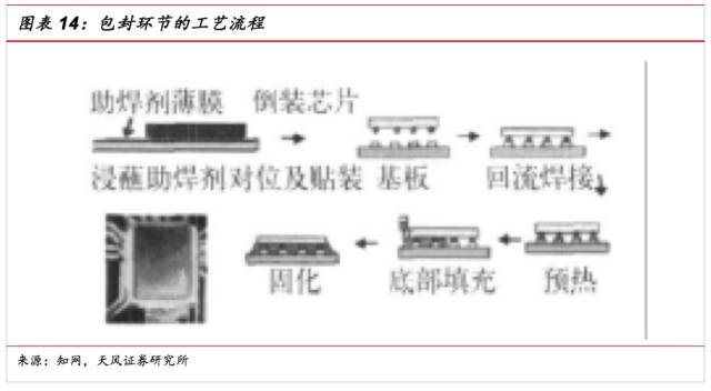
3SiP - born for applications
3.1. Main application areas
SiP has a wide range of applications, including: wireless communications, automotive electronics, medical electronics, computers, and military electronics.
The most widely used wireless communication field. SiP is the earliest and most widely used field in wireless communication. In the field of wireless communications, requirements for functional transmission efficiency, noise, volume, weight, and cost are increasingly high, forcing wireless communications to develop in the direction of low cost, portability, multi-function, and high performance. SiP is an ideal solution that combines the advantages of existing core resources and semiconductor manufacturing processes to reduce costs and time to market, while overcoming difficulties in SOC such as process compatibility, signal mixing, noise interference, and electromagnetic interference. The radio frequency power amplifier in the mobile phone integrates the functions of the frequency amplifier, power control, and transceiving switch, and is completely solved in the SiP.
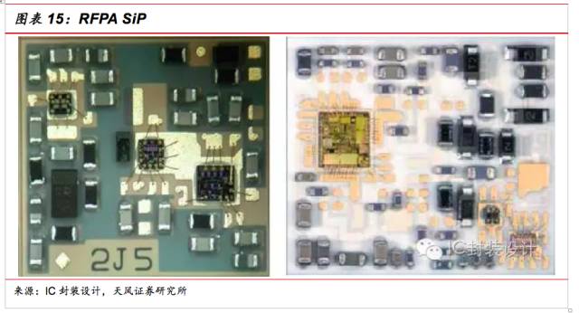
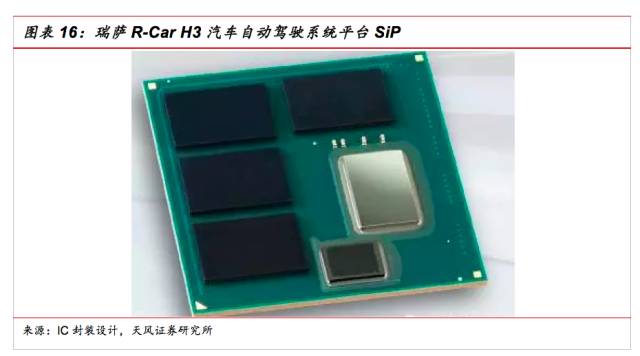
Automotive electronics is an important application scenario for SiP. The use of SiP in automotive electronics is gradually increasing. Taking the example of an engine control unit (ECU), the ECU consists of a microprocessor (CPU), memory (ROM, RAM), input/output interface (I/O), analog-to-digital converter (A/D), and reshaping, driving, etc. Scale integrated circuits. Different types of chips have different processes. At present, SiP is used more and more to integrate the chips into a complete control system. In addition, anti-lock braking system (ABS), fuel injection control system, airbag electronic system, steering wheel control system, tire low air pressure alarm system and other units, the use of SiP is also increasing. In addition, SIP technology has also been successfully applied in the rapidly growing automotive office systems and entertainment systems.
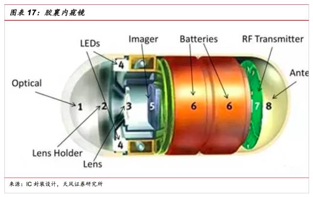
Medical electronics require a combination of reliability and small size, while providing both functionality and longevity. Typical applications in this field are implantable electronic medical devices such as capsule endoscopes. The endoscope consists of an optical lens, an image processing chip, a radio frequency signal transmitter, an antenna, a battery, and the like. The image processing chip belongs to the digital chip, the RF signal transmitter is an analog chip, and the antenna is a passive device. Concentrating these devices in one SiP can perfectly solve the performance and miniaturization requirements.
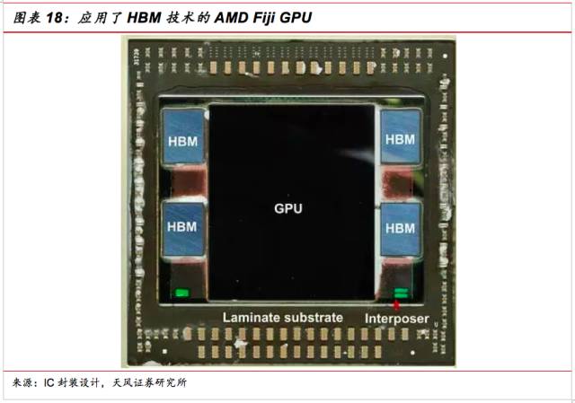
The application of SiP in the computer field mainly comes from integrating the processor and memory together. Taking GPU as an example, it usually includes a graphics computing chip and SDRAM. The packaging of the two is not the same. Graphical calculations are all packaged in a standard plastic ball array multi-chip package, which is not suitable for SDRAM. Therefore, after the two types of chips need to be separately packaged, they are packaged together in the form of SiP.
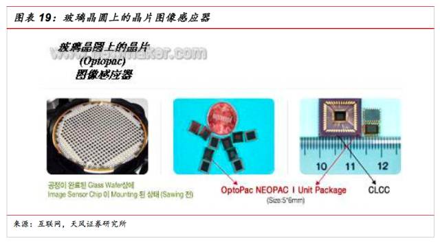
SiP also has many applications in other consumer electronics. This includes ISPs (image processing chips), Bluetooth chips, and more. The ISP is a core device for digital cameras, scanners, cameras, toys, and other electronic products. It converts optical signals into digital signals through photoelectric conversion, and then implements image processing, display, and storage. The image sensor includes a series of different types of components, such as CCD, COMS image sensor, contact image sensor, charge-loading device, optical diode array, and amorphous silicon sensor. SiP technology is undoubtedly an ideal packaging technology solution.
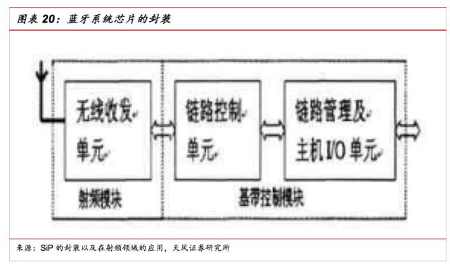
The Bluetooth system is generally composed of a wireless part, a link control part, a link management support part, and a main terminal interface. The SiP technology can make Bluetooth become smaller and smaller to meet the needs of the market, thus strongly promoting the application of Bluetooth technology. SiP completes all the originals (radio, baseband processor, ROM, filters, and other discrete components) needed to integrate Bluetooth wireless technology functions in an ultra-small package.
Military electronic products are characterized by high performance, miniaturization, variety, and small batch size. SiP technology complies with the requirements of military electronics applications, and therefore has a wide range of application markets and development prospects in this technology field. SiP products involve military equipment such as satellites, launch vehicles, aircraft, missiles, radars, and supercomputers. The most typical application products are transceiver components of various frequency bands.
3.2.SiP - Tailored for Smartphones
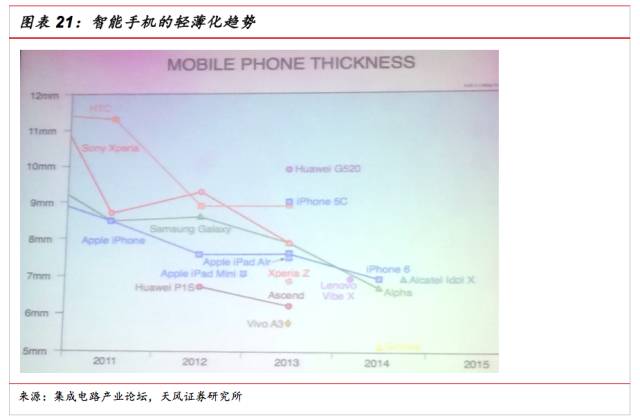
The thinning of mobile phones has brought about an increase in demand for SiP. Mobile phones are the largest market for SiP packaging. As smart phones become thinner and lighter, the demand for SiP is naturally rising. From 2011-2015, the thickness of all brands of mobile phones is continuously shrinking. Thinning naturally has higher and higher requirements for the thickness of the assembled parts. Taking the iPhone 6s as an example, the use of PCBs has been greatly reduced. Many chip components will be implemented in the SiP module. By the time of the iPhone 8, it is possible that Apple will use the SiP phone as the first device on the whole machine. This means that the iPhone 8 can be made lighter on the one hand, and there will be more room for other functional modules such as more powerful cameras, speakers, and batteries.
See SiP applications from Apple products. Apple is a company that firmly believes in SiP applications. Apple has used SiP packages on Apple Watch before.
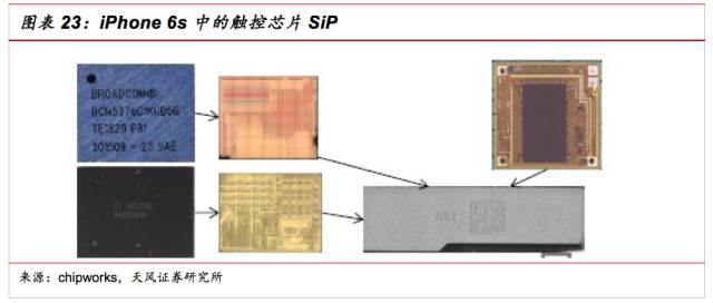
In addition to watches, the number of SiPs used in Apple phones is also increasing. Listed are: touch chip, fingerprint identification chip, RFPA and so on.
Touch chip. In Iphone6, there are two touch control chips, which are provided by Broadcom and TI respectively. In 6S, these two chips are sealed in the same package and the SiP package is implemented. In the future, TDDI will be further packaged together. iPhone6s shows a new generation of 3D Touch technology. The touch sensing detection can penetrate the insulating material housing and can detect the touch action of the human finger by detecting the voltage change brought by the human finger, thereby realizing different functions. The touch chip is to collect the voltage value of the contact point, convert the electrode voltage signal into a coordinate signal after processing, and control the mobile phone to perform the corresponding function response according to the coordinate signal, so as to achieve its control function. The emergence of 3D Touch puts forward higher requirements on the processing capability and performance of the touch module. The complex structure requires the touch chip to adopt SiP assembly, and the haptic feedback function enhances its operation friendliness.
Fingerprinting also uses SiP packages. The sensor and control chip are packaged together, starting from the iPhone 5, and similar technologies have been adopted.
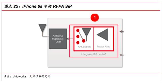
RFPA module. The RFPA in mobile phones is the most commonly used form of SiP. The iPhone 6S is no exception. In the iPhone 6S, there are multiple RFPA chips, all using SiP.

According to Apple's habit, all mature technologies will be passed on to the next generation. We judge that the upcoming Apple iPhone 7 will adopt SiP technology more, and the future iPhone 7s and iPhone 8 will be more comprehensive and use SiP technology to a greater extent. To achieve the compression of the internal space.
4 Rapidly growing SiP market
4.1. Rapid increase in market size and penetration
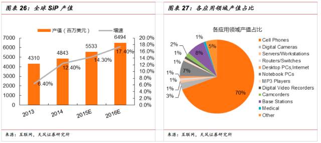
2013-2016 SiP market CAGR=15%. In 2014, the global SiP output value was approximately US$4.843 billion, which represented a growth of 12.4% from 2013. In 2015, with the continued growth of smart phones and wearable products such as Apple Watch, the global SiP output value is estimated to reach US$5.533 billion, which is higher than 2014. It grows 14.3% annually.
In 2016, although smart phones may gradually enter the mature stage and there is no significant growth performance, SiP may still show growth trend as applications become more popular. Therefore, it is estimated that the global SiP output value in 2016 will remain It can grow 17.4% over 2015 and come to 6.494 billion U.S. dollars.
Market penetration will increase rapidly. We expect that the penetration of SiP in smartphones will rapidly increase from 10% in 2016 to 40% in 2018. In the light of the thinning trend has been identified, SiPs that can achieve the perfect thin and light requirements should have more applications. More than Apple, we expect domestic smart phone manufacturers to follow up quickly. In addition, the increase in penetration will not only increase the use of SiP smartphones, but also increase the number of SiPs used in smart phones. The combination of the two effects drove the incremental market of SiP to expand rapidly.
We estimate the market size of SiP in the smart phone market in the next three years. Assuming that the unit price of SiP is reduced by 10% annually, smartphone shipments will increase by 3% annually. It can be seen that the new market size of SiP in smart phones is CAGR=192%, which is very impressive.

4.2. From manufacturing to packaging and testing - gradually integrated SiP industry chain
From the perspective of the changes in the industrial chain and the changes in the industrial structure, the future electronic industry chain will no longer be just a traditional vertical chain: terminal equipment manufacturers - IC design companies - packaging and testing companies, Foundry plant, IP design company, product The design will simultaneously mobilize the packaging vendors, substrate manufacturers, material factories, IC design companies, system vendors, Foundry factories, device manufacturers (such as TDK, Murata), and storage giants (such as Samsung) to collaborate with each other to jointly realize industrial upgrading. In the future, the system will drive the further development of the packaging industry, whereas the high-end packaging will also promote the prosperity of the system terminal. In the future, the direct connection between system manufacturers and packaging factories will be more and more, and IC design companies will probably develop in two directions: IP design or direct sales of wafers.

In recent years, some foundries have also started to expand their services to the downstream packaging industry with their turnkey service requirements. They are developing SiP and other advanced packaging technologies to build a one-stop service model to meet the upstream IC design. Factory or system factory. However, the foundry's advanced packaging technology such as SiP will form a delicate competitive relationship with existing packaging and testing companies. First, the wafer foundry is based on the advantages of wafer processing and has the basic conditions for developing wafer-level packaging technology. The threshold for entry is not very high. Therefore, according to the trend of product application and the needs of upstream customers, the wafer foundry can continue to move toward wafer-level packaging and other subsequent segments after completing the wafer foundry-related processes to complete the overall customer demand. This may create a certain level of competition for existing packaging and testing companies.
Since it is almost impossible for the packaging and testing plants to go upstream to the wafer foundry industry, the foundry can step into the downstream packaging and testing OEM based on the advantages of process technology, especially in the high-end SiP field; therefore, the foundry Into the SiP packaging business, we will switch from a purely upstream-downstream partnership to a subtle competing relationship.
On the one hand, packaging and testing plants can be differentiated and developed to differentiate between markets. On the other hand, they can also choose to conduct technical cooperation with foundries, or use technology licenses, etc., with the huge production capacity of packaging and testing plants to carry out orders. Production, and jointly expand the market. In addition, the high-level heterogeneous packaging developed by the foundry, part of the process steps still need professional sealing and testing plants to assist with the completion of existing technologies, so the two sides still have a cooperation base.
4.3. SiP industry standard
Moonlight + Universal Electronics:
In the world's major packaging and metering manufacturers, Sunlight and Moonlight purchased the Electronic Foundry Service (EMS), Huanxu Electronics, as early as in 2010, and used its own packaging technology to match the strength of the loop design and system integration to develop SiP technology. Sun Moonlight has maintained its leading position in SiP technology and has been able to obtain orders from mobile phone makers such as Wi-Fi, processors, fingerprint recognition, pressure touch, MEMS and other modules, which will provide future growth drivers for the company.
In addition, the company also developed a TSV 2.5D IC technology in the SiP category with its strategic alliance with a DRAM manufacturing giant Inacore. Huawei Technologies Co., Ltd. provided Silicon Interposer silicon wafers to manufacture and manufacture solar wafers. Step-by-step measurement and measurement capabilities, expanding the existing package product line of Sun Moonlight.
Not only that, the company also cooperated with Japanese substrate manufacturer TDK to establish a subsidiary company, Riyueyang, to produce integrated circuits with embedded substrates, allowing more sensors and RF components and other chips to be integrated on smaller-sized substrates. SiP power is reduced in energy consumption and is smaller in size to meet the needs of wearable devices and the Internet of Things.
The major growth drivers for the company will come from SiP. The 1H2016 SiP revenue is nearly 2 billion U.S. dollars. It is expected that SiP will be the driving force for the company's continued growth in the next 5-10 years. Sun & Moon Electronics’ subsidiary, Huanxu Electronics, won the order of SiP, the second US-based smartwatch, after it took down A’s wearable watch, SiP, and is scheduled to ship next year.
Security:
The second largest sealing and measuring plant in the world is the South Korea factory site as the main base for the development of SiP. Except 2013
The company has invested in South Korea for over a year to build advanced plants and a global R&D center. Anh Si currently uses SiP technology mainly for image sensors and motion sensors. According to the Q2 2016 financial report, the demand for WLCSP and SiP from Chinese high-end smartphones is the main driving force for the company's growth.
Product:
The third largest product in the world, Taiwan's second largest sealing and testing factory, is the layout of IC-integrated SiP. The main focus is on fan-type package (FO PoP) technology. It is mainly used in smart phones, and it is currently part of the two sides of the Taiwan Strait. Mobile phone chip maker cooperation is expected to be officially mass-produced in 2016.
Due to the lack of module design and system integration, counterfeit products are actively seeking honours with EMS Dachang Hon Hai strategic alliance in order to combine the company's ability in module design and system integration to make the SiP technology field more complete.
Long Power + Star Branch Jin Peng:
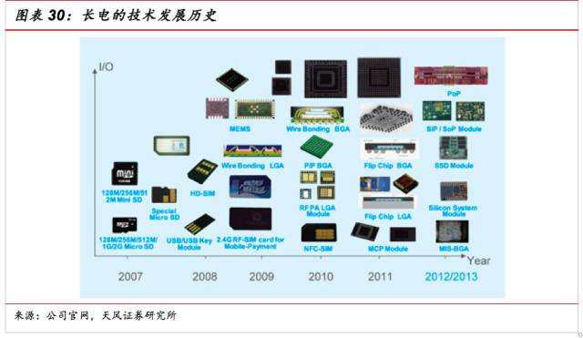
Changde is one of the few semiconductor packaging and testing companies in China that can meet the international technological standards. In 2015, it joined hands with SMIC and the National Fund to purchase Singapore Starbucks for US$780 million. Global rankings went from sixth to fourth. The company has certain technical advantages in SIP packaging and has successfully developed a series of products such as RF-SIM, Micro SD, USB, FC-BGA and LGA module.
StarTech Jinpeng, previously ranked as the world’s fourth-largest maker of sealing and testing equipment, is also actively developing SiP technology at the Korean plant. However, due to the overall operating conditions being inferior to the top three manufacturers, it is difficult to invest large amounts of capital to expand the SiP scale. However, with the acquisition of Jiangsu Changjiang Power's acquisition of Xingke Jinpeng, it will be able to combine Siemens Jinpeng's technology and continue to expand SiP. Changjiang Electronics will invest 475 million US dollars to expand the SiP project. At present, Xingke Jinpeng Korea Plant has been officially mass-produced, and its capacity utilization rate is over 95%, mainly for A customers. We expect that in the future, as the amount of SiP in the A customer BOM increases, it will bring great flexibility to the company.
5 recommended logic
SiP represents the development direction of the industry. The development of the chip from blindly pursuing the decline in power consumption and performance (Moore's Law), to more pragmatic to meet market demand (surpassing Moore's Law), SiP is an important path to achieve. SiP from the point of view of terminal electronic products, not just concerned about the performance/power consumption of the chip itself, but to achieve the entire terminal electronic products, slim, thin, multi-functional, low power consumption, after the rise of lightweight products such as mobile devices and wearable devices, SiP demand is increasingly apparent.
The penetration rate of SiP in smart phones is increasing rapidly. The CAGR of the SiP market 2013-2015 reached 16%, which is higher than the 7% CAGR of the smartphone market. With the determination of the slimming trend of smart phones, the penetration rate of SiP will increase rapidly and is expected to increase from the current 10% to 40% by 2018. We emphasize that we must pay attention to any new changes in smart phones, and before they reach 40% penetration, they are all worthy of attention.
From the perspective of industry configuration, SiP has not yet been fully priced in and has room for growth. In the Q2 financial report, Safe and Sunlight and Moonlight, one of the reasons for the increase in the chain ratio, comes from the volume of SiP packaging. At the same time, Apple decided to use multiple SiPs in the new model, and domestic manufacturers have not yet begun to keep up. We estimate that the potential SiP incremental space in 2018 is US$9.6 billion. From the perspective of industry configuration, the growth of SiP has not yet been fully recognized by the market and there is enough room for growth. We believe that among the listed companies in China, Changjiang Electronics (the acquired Star Jinpeng will provide SiP products for A customers) and Huanxu Electronics (Apple watch SiP supplier) will benefit from the development of the SiP industry in depth.
P2.2X3 Automotive Right Angle Male Connector
P2.2X3 Automotive Right Angle Male Connector.Automobile connector is a kind of component that electronic engineers and technicians often contact. Its function is very simple: build a communication bridge between blocked or isolated circuits in the circuit, so as to make the current flow and realize the predetermined function of the circuit. The form and structure of automobile connector are ever-changing. It is mainly composed of four basic structural components: contact, shell (depending on the variety), insulator and accessories.
P2.2X3 Automotive Right Angle Male Connector
ShenZhen Antenk Electronics Co,Ltd , https://www.antenkconn.com