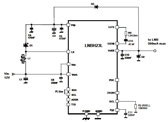
The LNBH23L monolithic voltage regulator is designed to provide a 13/18 V power supply and a 22 kHz audio signal for the LNB downconverter. The IC can be designed with a very simple high efficiency LNB power supply LNBH23L monolithic voltage regulator and interface. Antenna reflector or multi-switch box. The LNB power supply circuit provides a very low component count, low power consumption combined with a simple design and a complete solution for the I 2 C standard interface.
The design of this LNB power supply is very simple and requires very few external components. The LNBH23L regulator has a built-in DC-DC boost converter that generates a voltage (VUP) from a single source from 8 V to 15 V: allowing the linear post regulator to operate at a minimum power consumption of 0.55 W TYP. @500 mA load. The undervoltage lockout circuit will reduce the VCC provided when the entire circuit is disabled below a fixed threshold (typically 6.7 V).
Some of the features in this power supply circuit diagram: auxiliary modulation input, accurate built-in 22 kHz tone generator suit, overload and over temperature with my internal protection 2 C diagnostic bit, LNB short circuit dynamic protection.

Jiangsu Qilong Electronic Technology Co., Ltd. , https://www.jsqldzkj.com