FPGA (Field-Programmable Gate Array), field programmable gate array, which is the product of further development based on PAL, GAL, CPLD and other programmable devices. It appears as a kind of semi-custom circuit in the application-specific integrated circuit (ASIC) field, which not only solves the defect of the custom circuit, but also overcomes the shortcomings of the original programmable device with a limited number of gates.
The main difference between FPGA and CPLDBack in the mid 1980s, FPGAs had taken root in PLD devices. CPLDs and FPGAs include a relatively large number of editable logic cells. CPLD logic gates have a density of between a few thousand and tens of thousands of logic cells, and FPGAs are typically in the tens of thousands to millions.
The main difference between CPLDs and FPGAs is their system architecture. CPLD is a somewhat restrictive structure. This structure consists of a logical group of one or more editable sums and a relatively small number of locked registers. The result is a lack of editing flexibility, but it has the advantage of predictable latency and a high ratio of logical units to connected units. FPGAs, on the other hand, have a lot of connection units. This makes it more flexible to edit, but the structure is much more complicated.
Another difference between CPLD and FPGA is that most FPGAs contain high-level built-in modules (such as adders and multipliers) and built-in memory. Therefore, a related important difference is that many new FPGAs support full or partial in-system reconfiguration. Allow their design to change as the system upgrades or dynamically reconfigures. Some FPGAs allow a portion of the device to be re-edited while others continue to operate normally.
There is one difference between CPLD and FPGA: After the CPLD is powered off, the original burned-in logic structure will not disappear. After the FPGA is powered off, when it is powered on again, it needs to reload the logic code inside the FLASH, which requires a certain loading time.
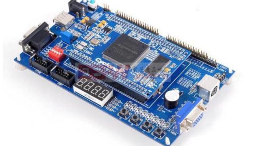
FPGA adopts the concept of logic cell array LCA (Logic Cell Array), including three parts: configurable logic block CLB (Configurable Logic Block), output input block (IOB) and internal interconnect (Interconnect).
Compared with traditional logic circuits and gate arrays (such as PAL, GAL, and CPLD devices), FPGAs have different structures. FPGAs use small lookup tables (16 & TImes; 1 RAM) to implement combinatorial logic. Each lookup table is connected to a D flip-flop. At the input, the flip-flop drives the other logic circuits or drives the I/O, and thus constitutes a basic logic unit module that can realize both the combinational logic function and the sequential logic function. These modules are connected or connected by metal wires. To the I/O module.
FPGA logic is implemented by loading programming data into internal static memory cells. Values ​​stored in memory cells determine the logic functions of logic cells and the connection between modules or modules and I/O, and ultimately determine the FPGA can realize the function, FPGA allows infinite programming.
The significance of FPGA in next-generation network architectureThis will focus on the role and significance of FPGAs in virtual network architectures such as NFV.
Telecommunications network is a major application scenario of NFV. One of the most direct motivations for its emergence is to support exponential bandwidth growth. It is predicted that global IP traffic will grow by more than three times today compared to today. In today's Internet of Things, especially when technologies such as 5G, Internet of Things, and autonomous driving have become the focus of competition among major companies, various equipment and services require telecommunication networks and their data centers for processing and support. However, the traditional telecom infrastructure and data center are difficult to effectively expand. The main reasons are as follows:
Hardware level: The traditional telecommunication network infrastructure uses various types of dedicated hardware devices, such as various access devices, switches, routers, firewalls, and QoS. There are many problems in doing so, for example, poor compatibility between different devices, difficulty in maintenance upgrades, easy monopoly by suppliers, drastic increase in costs, development of new hardware devices if new features are needed, and so on.
Software level: Different devices need their own corresponding software to configure and control, which makes it difficult to implement a large-scale uniform deployment and configuration at the administrator level, and it is necessary to learn software configuration methods from different vendors and specifications. If some network functions are implemented through software, the effective utilization of the server in the traditional implementation method is very low, and the dynamic migration of the service cannot be performed.
Therefore, virtualization technology - more specifically, network function virtualization NFV technology, has gradually become an effective way for major operators to solve the above problems. The European Telecommunications Standards Institute (ETSI)'s more famous schematic diagram of NFV is shown below.
In general, NFV uses common servers (mostly based on Intel x86 processors), general-purpose storage devices, and general-purpose Fast Ethernet switches to implement various network functions of traditional telecommunications network infrastructures compared to traditional methods. Specifically, the network function is implemented in software in a general-purpose server, data is stored using a common storage device, and network traffic is forwarded through a general-purpose network card and a high-speed switch. This can theoretically solve the above-mentioned problems at the hardware level: The use of general-purpose devices instead of dedicated devices will increase the scalability of the data center and will not be constrained by a certain supplier. Instead, it will reduce hardware procurement and deployment through open competition. the cost of.
In addition, with virtualization technology, network functions are implemented in different virtual machines. This theoretically solves the problem at the software level: that is, a specific application does not occupy all the resources of the server. Conversely, a server can run multiple virtual machines at the same time. Machine or network service. At the same time, the expansion and migration of virtual machines in the data center is also more convenient and will not result in service downlines or interruptions.
NFV and another technology: Software Defined Network (SDN) often appear together. One of their main core ideas is to separate the control plane and the forwarding plane of the network. In this way, all data forwarding plane devices can be controlled, configured, and managed at the same time, thus avoiding the inefficiency of administrators needing to configure each network device individually.
Quoting "China Telecom CTNet2025 Network Architecture White Paper":
"From the perspective of better adaptation to Internet applications, the future network architecture must require the opening and standardization of network capability interfaces. Through software-defined network technologies, it is possible to realize the scheduling and customization of business-oriented network resources and capabilities, and to accelerate further. With the platform of network capabilities, it is also necessary to provide network-programmable capabilities to truly realize the deep openness of network services.
Please note that I used a lot of "theoretical" in the previous statement. This is because many of the advantages of NFV above are people's good imagination and vision. In practical engineering practice, designing and implementing an effective NFV architecture faces many problems. For example, in different application scenarios, the types of network loads vary, and many applications require line-rate processing such as QoS and traffic shaping (previously described in the blog post), VPN, firewall, network address translation, encryption and decryption, and real-time processing. Monitoring, Deep Packet Inspection (DPI) and more. Even if there is a dedicated software development library such as DPDK, it is technically difficult to use the software to implement the wire speed processing of these network services. The network functions implemented by software are difficult to compare with the proprietary hardware. As a result, people will in turn question the starting point and motivation for using NFV. At the same time, given that NFV is still in the phase of program exploration and exploration, many related agreements and standards have not yet been determined, which, to a certain extent, makes many companies hesitate to invest a lot of resources in the preliminary investigation work.
Therefore, how to effectively implement these virtualized network functions (Virtualized Network FuncTIon - VNF) is the main task of our previous stage and the main issues discussed in this white paper.
Effective Implementation of Virtual Network Function (VNF)Here, the "effectiveness" of implementing virtual network functions is mainly reflected in the following aspects:
1.VNF must be very flexible and easy to use;
2. Easy to scale up, not limited to a certain application scenario or network;
3. Performance should not be lower than or even higher than dedicated hardware.
Here, the white paper gives several potential directions for reference:
1. The separation and independent expansion of the control plane and the forwarding plane.
2. Design and optimize and standardize the forwarding surface with programmable capabilities.
In the application scenario of the telecommunication network, a typical application of NFV is the virtualized broadband remote access service vBRAS (virtual broadband remote access server, also referred to as vBNG, virtual broadband network gateway). VBRAS may include many virtual network functions, such as Remote Authentication (DRA), Dynamic Host Configuration Protocol (DHCP), and DPI and firewall mentioned previously. , QoS, etc.
An important discovery is that these network applications can be divided into two categories from the requirements of computing resources. One type does not require a large amount of computing resources such as RADIUS and DHCP. At the same time, many of these applications belong to the control plane. Therefore, this type of application is suitable for being placed directly on the control plane and has good vertical and horizontal scalability. It is also very suitable for implementation with general-purpose computing and storage devices.
Another type of application often requires a lot of computing power, such as traffic management, routing forwarding, data packet processing, etc., and it usually needs to be processed at an online speed (such as 40 Gbps, 100 Gbps, or higher). Such applications often belong to the data plane. For the data plane, it also needs to support a large number of network functions with large amounts of computation, so as to distinguish it from the use of proprietary hardware and meet the original intention of the NFV technology. To sum up, the data plane should have the following two main capabilities:
1. Ability to handle high-throughput complex data packets at wire speed;
2. Supports multiple network functions at the same time, with strong programmability.
However, if the software method is used directly, these two functions are difficult to satisfy at the same time. Therefore, we have adopted FPGA as a smart hardware acceleration platform, which has solved both the processing speed and programmability problems. First of all, FPGAs have absolutely superior hardware parallelism in packet processing compared to software-only methods and are therefore used as hardware accelerators. Second, compared to traditional proprietary hardware devices, FPGAs have a flexible programmability that can support the implementation of various applications.
Virtual Broadband Remote Access Service: Evolution from BRAS to vBRAS
Figure 1: Evolution of vBRAS
The figure above shows us the three main processes of the gradual evolution of traditional BRAS to vBRAS:
1. In the first stage, the traditional BRAS uses dedicated equipment and the control plane and the forwarding plane are tightly coupled. The figure shows that the control path and the data path are coincident.
2. In the second phase, virtualization technology was adopted, and the server was replaced with a dedicated BRAS device, and multiple vBRASs were implemented using software and virtual machines. However, it can also be seen that the control plane and the forwarding plane are still coupled to each other. Since the performance of the two is very different, this implementation method can easily cause performance bottlenecks in the data path, or occupy the bandwidth of the control plane because the data path traffic is too large. Conversely, the flow at the control plane affects the ability of the wire speed packet processing on the data plane.
3. In the third stage, virtualization technology is adopted, and the control plane and the forwarding plane are separated from each other. As can be seen from the figure, the control plane and the forwarding plane are implemented separately by two servers, and the control traffic and the forwarding traffic do not affect each other. In addition, control traffic can flow in both directions between the data/forwarding server and the control server, enabling control to control the forwarding plane.
This third phase is the latest result of joint R&D by Intel, HPE and China Telecom North Research Institute. Next, we will explain in detail the technical details.
High-performance vBRAS design methodDesigning and implementing the high-performance vBRAS solution in the third stage above requires the implementation of vBRAS-c (control) and vBRAS-d (data), that is, vBRAS control devices and vBRAS data devices. Both types of equipment should be implemented using standardized, general-purpose servers. In addition, for vBRAS data devices, special optimization and acceleration are required for applications with a large amount of calculations to enable high-throughput and low-delay packet processing.
The following figure shows the design method for vBRAS-c and vBRAS-d in this application example.
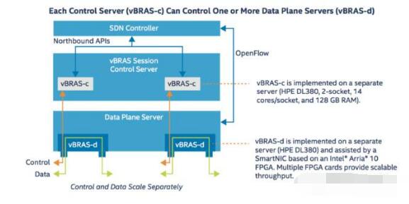
Figure 2: VBRAS transfer control separation architecture
For the vBRAS-c node, its important design idea is lightweight and virtualization, which makes it easy to expand and transplant in the data center or cloud, and can be distributed to control multiple data plane nodes. So in this example, vBRAS-c is implemented by a standalone HPE DL380 server. The DL380 server contains two CPU sockets, each with a 14-core Xeon processor. The total memory of the server is 128GB. In terms of network interfaces, vBRAS-c can use standard network cards for network communication. For example, one or more Intel X710 10GbE network cards can meet the control plane traffic requirements. The specific vBRAS control application is implemented in the virtual machine. Multiple virtual machines are controlled by the SDN controller.
For the vBRAS-d node, the overall implementation is also through a separate DL380. For the above-mentioned optimization acceleration part, an Arria 10 FPGA-based intelligent network card acceleration network function is used in this example, such as line-rate processing QoS and multi-level traffic shaping. In a DL380, multiple FPGAs can be inserted to implement parallel data processing and multiply data throughput. At the same time, the vBRAS-d node interacts with the SDN controller through OpenFlow, and one vBRAS-c device can control multiple vBRAS-d devices.
Intelligent NIC Resolution Based on Arria10 FPGAThe benefits of using an FPGA smart network card for network acceleration include the following:
1. Liberated valuable CPU cores, offloaded data processing originally implemented in the CPU onto the FPGA for accelerated implementation. In this way, the CPU can be used for other tasks, and the effective use of resources can be further realized on the basis of virtualization.
2. FPGAs have low power consumption and are flexible and programmable. As mentioned in the white paper, hardware QoS and multi-level traffic shaping on the selected Arria 10 GT1150 device consume only 40% of the FPGA's logic resources. In other words, 60% of resources can be used for other network functions processing and acceleration. At the same time, the FPGA can be programmed at any time, so the acceleration of multiple network functions can be completed with a set of hardware devices without the need to replace accelerator cards or other hardware devices. Even a user-defined function can be implemented without a proprietary device. This is a good balance between high performance and high versatility.
3. FPGA can process high-speed parallel data packets, and it is widely used in the field of network communications. The solution is rich and mature.
The following figure outlines the data path design for packet forwarding implemented in the FPGA in this example.

Figure 3: Data Paths for FPGA Packet Processing
As can be seen from the figure, the design includes multiple modules, such as Parser, Look-Up, Buffer Manager, Packet Processor, and memory controller and DMA. After the data packet enters the FPGA, it performs feature extraction, classification, and search through each module in turn, and if necessary, interacts with the CPU through PCIe and DMA. At the same time, the Buffer Manager performs traffic control, QoS, and traffic shaping operations on packets from different sources.
In addition, this FPGA intelligent network card supports a variety of packet processing modes, that is, the data packet can be completely processed in the FPGA and then forwarded without passing through the CPU; it can also send data packets to the CPU through the PCIe, use the DPDK for packet processing, and then through FPGA forwarding; or a combination of the two, some of the functions are implemented in the CPU, and the other is offloaded to the FPGA. Visibility is high.
Performance Testing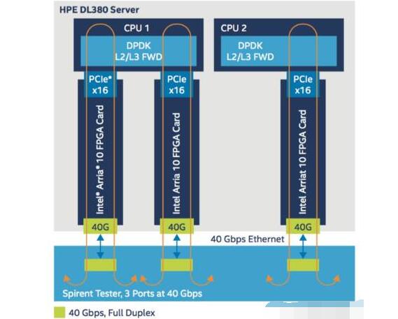
Figure 4: Data plane server and FPGA architecture
As can be seen in the figure, one DL380 server is plugged with three independent FPGAs and each network adapter supports 40Gbps data throughput. Therefore, the total throughput supported by one vBRAS-d server is 120Gbps. Each network card is connected to the CPU through the PCIex16 interface. The DPDK L2/L3 FWD application is run in the CPU, and the data is forwarded back to the FPGA. Then QoS and data shaping are performed in the FPGA. During the test, both the generation and receipt of the flow were achieved with the Spirent tester.
For QoS, each intelligent network card can support 4000 users, so a single server supports 12,000 users. Each user supports 2 priorities, and the bandwidth allocated to each user can be programmatically controlled. For example, if each user allocates 8.5 Mbps bandwidth, the total traffic of the single server should be 12000 x 8.5 = 102 Gbps after traffic shaping is enabled, as shown in the following figure.
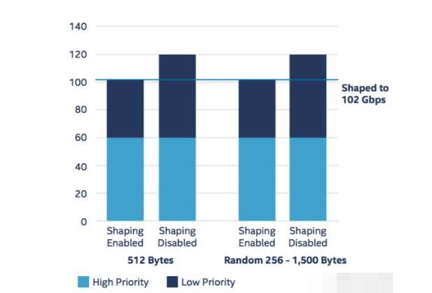
We see that when the packet is 512 bytes in length, traffic shaping does not affect the loss of both high-priority traffic and low-priority traffic, each at 60 Gbps (5 Mbps high priority for each user's actual traffic). +5Mbps low priority), so the total traffic is 120Gbps. After traffic shaping is enabled, high-priority traffic is not lost, and it is still 60 Gbps. For low priority, since each user allocates 8.5 Mbps bandwidth and high priority already occupies 5 Mbps, only 3.5 Mbps bandwidth remains for low-priority traffic to pass through. It can be seen that low-priority traffic is subject to traffic limiting, and the total traffic becomes 3.5Mx12000=42Gbps, making the total traffic 102Gbps. This proves in general that a single vBRAS-d node can support more than 100Gbps traffic processing.
In addition, some power consumption test performance comparisons have been made. Here I have selected a result chart as shown below.
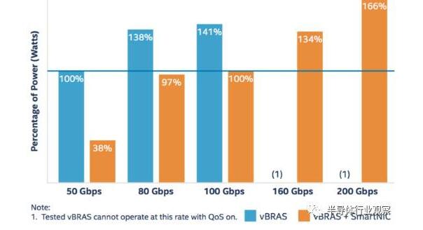
Figure 5: Comparison of total energy performance ratios at different bandwidths
This figure shows a series of comparisons of the total power performance ratio when implementing different bandwidths. The power performance ratio is defined as the total power consumption (kW) required to achieve 1 Tbps. In the figure, the power consumption performance ratio at 50 Gbps for vBRAS without an FPGA intelligent network card is used as a reference value (100%). As can be seen from the figure, the vBRAS+FPGA smart card solution can always reduce total power consumption by more than 40%, up to 60%. This further confirms the benefits of using FPGAs to accelerate network functions as explained above.
Other performance tests and comparisons will not be repeated. Details can be found in the white paper. Overall, compared to the traditional vBRAS server + standard network card solution, the solution using vBRAS + FPGA intelligent network card can reduce power consumption by about 50%, and bring more than 3 times the performance improvement.
SWOT four dimensions to analyze the current domestic development of FPGA prospects(1) First say the advantages. Compared to xilinx and altera, domestic FPGA manufacturers currently have no absolute advantage, only comparative advantages, such as a high starting point, no longer need to start from the micron technology, from the beginning to enter from tens of nanometers, the process gap can be reduced to 2- The level of 3 generations. In addition, China is a large country of application of FPGA chips. Domestic FPGAs have various advantages of localization, such as the understanding of the needs of small and medium-sized customers, etc., which are more grounded than foreign giants.
(2) Weaknesses Obviously, there are significant gaps between domestic FPGA manufacturers and foreign giants, from patents, technical products to talents and market brands.
(3) Speaking of opportunities, Chinese companies currently face more opportunities, because at the national level, FPGAs have been listed as national strategic chips, and the government’s investment in this area may gradually increase. Although the government directly controls the development of this industry may not be A good way, but it is very important to give support to the private sector in all aspects. In addition, with the development of China’s economy, Chinese companies can attract more and better international talents, especially some high-end FPGA talents, which are crucial to the development of a company. Finally, with the development of emerging industries such as artificial intelligence and big data, the market capacity of FPGAs may experience large-scale growth.
(4) Finally say threats. When it comes to threats, the patent is one. When Chinese companies are still very weak and far from composing for the international giants, the risk is not great. If a competitive relationship is already formed, the giants may take up their patented weapons to defend their own interests, like ZTE, Huawei's problems in the development process are the same. This requires China's FPGA manufacturers to work hard and build up patents and technologies to meet future patent warfare and internationalization. Otherwise, Making a product may not be far off.
Overall, although China currently has a large gap in this field of FPGAs compared with foreign mainstream manufacturers, considering the development of China’s economy and the increase of comprehensive national strength and the government’s high regard for the chip industry, there is also a possibility that this market may emerge. With a substantial increase, the gap between China's domestic FPGAs and foreign mainstream manufacturers will gradually narrow. Although this process will be relatively long, the trend is undoubted.
In recent years, several FPGA manufacturers have been born in China. For example, Beijing Micro Accord, Anlu, Tongchuang and Gaoyun Semiconductor have all launched their own FPGA chips, some of which are already in commercial use and some are in large companies. This is a good signal for sample identification and testing projects. In this year's "IC-CHINA 2017" conference, Gao Yun released three new products, not only the SOC FPGA with ARM3 integration, but also the "Chenxi" series based on the 55nm SRAM technology and the 55nm embedded Flash + SRAM. "Bees" 4 series of 11 products, basically covering the lattice 70% ~ 80% of the products, especially small bee series, corresponding to lattice XO2/XO3, to form a strong alternative competitive advantage. In addition, Gaoyun's 28nm product is already under development and is expected to be launched around 2019. Currently, the cumulative shipments of Gaoyun FPGA chips are expected to reach 2 million pieces. For a company that has only been established for about 3 years, this development is very rapid. If the chip's yield rate is gradually increased in the application, the reliability of the chip is getting users. This recognition will have a great impact on foreign manufacturers. At the same time, An Road also released its latest 55nm second generation "elf" ELF2 series of high-performance low-power and embedded MCU SOC FPGA, launched a challenge to foreign manufacturers of low-end products.
Looking back at every well-developed industry in China, basically following a logic, first breaking through from the low end, replacing similar foreign products, and after the industry has established a stable foothold, it will continue to improve and continuously improve its own technology and products. After a certain period of time, we can create some requirements in the subdivided areas, and continue to make advances to the high-end, eventually occupying a place in the high end of the industry. China's telecommunications manufacturing industry, high-speed rail manufacturing, etc. all follow this logic. "Low-end Breakthrough -" Continuous Improvement - "Creating Demand - "High-End Leading" is the only way for China's various industries to develop. For the FPGA industry, it can also be developed in accordance with this idea.
The market prospect of FPGA is attractive, but the high threshold is unsurpassed in the chip industry. More than 60 companies have invested billions of dollars in the world and went to the summit of FPGAs. There are many industry giants such as Intel, IBM, Texas Instruments, Motorola, Philips, Toshiba, and Samsung. However, only the top ones succeeded. Four companies in Silicon Valley in the US: Xilinx, Altera, Lattice, and Microsemi. Among them, Xilinx and Altera share nearly 90% of the total. With a market share of more than 6,000 patents, the technical barriers posed by such a large number of technical patents are of course unattainable. Xilinx has always maintained the dominance of the global FPGA. Today, the semiconductor market has become a three-way situation, FPGA, ASIC and ASSP three worlds. Market statistics show that FPGAs have gradually eroded the traditional ASIC and ASSP markets and are in a period of rapid growth.
1.2 Inch Fnd Numeric Display,Indoor Fnd Numeric Display,Single Digit Fnd Numeric Display,1 Digit Fnd Numeric Display
Wuxi Ark Technology Electronic Co.,Ltd. , https://www.arkledcn.com