K214 / J77 single-ended headphone amplifier
The single-ended amplifier circuit is a model for changing the sound quality with efficiency. The circuit described below is a single-ended headphone amplifier made of FET and MOS tubes. It is suitable for driving medium and low impedance headphones with not too low sensitivity.
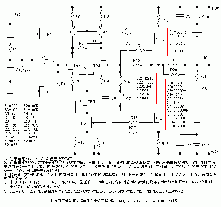
First, the circuit principle, as can be seen from the following figure, the entire amplifier can be divided into 4 parts: 
1. The buffer circuit composed of TR1 (K246) and TR2 (J103): used to isolate the signal interference between the front and rear stages and improve the clarity of the sound. This circuit is a class A complementary source output device with high input impedance. While the output impedance is very small, Japanese enthusiasts have applications in many circuits. Adjusting R3 can keep the output midpoint of the circuit around 0V.
2. Use a twin TR3, TR4 (NPD5566) to form a differential amplifier circuit: the advantage of using a twin field effect tube is that the symmetry of the tube is good, and the heavy and complicated matching work is omitted. The field effect tube can withstand a large dynamic input signal and keep in the class A working state under the condition of large current operation, and does not introduce high-frequency noise because of the increase of the working current. The quiescent current of this stage is about 9MA per tube. In order to cooperate with the high current working state of NPD5566, the load of the differential amplifier stage uses an active load, which is composed of Q1 (A1145) and Q2 (A1145) to form a mirror current source.
3. The output stage adopts K214 / J77 with mellow and delicate sound quality as the output stage, and the drain output configuration is adopted in the circuit.
4. The circuit of TR5 and TR6 (NPD5566) not only provides a constant current source load for the TR3 and TR4 differential circuits, but also provides a bias voltage for Q4, so that Q4 has a fixed working current, and provides a constant current source load for the output amplifier Q3 .
2. Working principle:
The input signal is coupled to the buffer stage through the input capacitor. After the buffer stage isolation, the input signal is input to the differential amplifier circuit, and the amplified signal drives Q3 to output to the load.
3. Installation and commissioning:
During the installation process, as long as the components are measured before welding and the welding is correct, there will be basically no problems. The focus is on the debugging process. The usual debugging process has 2 steps:
1. Adjust the precision adjustable resistor R3 to make the output potential closest to 0V. In the prototype made by the author, the output midpoint can be controlled within 10MV.
2. Adjust the resistance R11 so that the static current of the output stage is between 80-140MA. This current can be converted by measuring the voltage across the resistor R13 or R19, that is, the voltage across the resistor is: 0.26V-0.46v It has been proved by practice that the sound quality is clearer when the current is lower, and the sound quality is thicker when the current is larger. It can be adjusted according to personal preferences.
|


![[Photo] Top-of-the-line tube OTL headphone amplifier](http://i.bosscdn.com/blog/20/06/41/513328481.gif)

