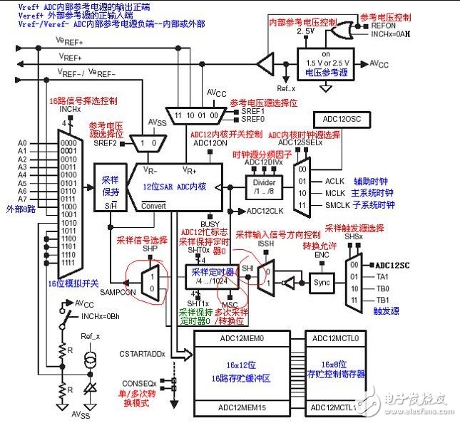
The ADC12 module consists of the following: 16 input analog switches (8 external, 4 internal), ADC internal voltage reference, ADC12 core, ADC clock source, acquisition and hold/trigger source, ADC data output Part, ADC control register and other components.
Four sampling modes:
(1) Single channel single conversion mode
(2) Sequence channel word conversion mode
(3) Single-channel multiple conversion mode
(4) Sequence channel multiple conversion mode
Personally think that the (3) model should be used more often.
Perform multiple conversions on the selected channel until the function is turned off or ENC=0. Make the following settings:
x=CSStartAdd, point to conversion start address
ADC12MEMx save conversion result
The channel and reference voltage are defined in the ADC12MCTLx register
In this mode, you can change the conversion mode without first stopping the conversion. After the conversion that is currently in progress, you can change the conversion mode. There are several ways to stop this mode:
Use CONSEQ=0 to change to single channel single mode.
Use ENC=0 to directly stop the current conversion.
Replace single mode single mode with current mode while ENC=0
ADC control register
ADC12CTL0 Conversion Control Register 0
ADC12CTL1 Conversion Control Register 1
ADC12IE Interrupt Enable Register
ADC12IFG Interrupt Flag Register
ADC12IV Interrupt Vector Register
ADC12MEM0-15 memory control register 0-15
ADC12MCTL0-15 Storage Control Register 0-15
The general approach: Start the conversion in the big loop, and the interrupt is triggered when the conversion completes. We record and process the conversion data in the interrupt.
Register Type Register Abbreviation Register Meaning
Conversion Control Register ADC12CTL0 Conversion Control Register 0
ADC12CTL1 Conversion Control Register 1
Interrupt Control Register ADC12IFG Interrupt Flag Register
ADC12IE Interrupt Enable Register
ADC12IV Interrupt Vector Register
Storage and Control Registers ADC12MCTL0 to ADC12MCTL15 Storage Control Registers 0 to 15
ADC12MEM0 to ADC12MEM15 memory registers 0 to 15
1. ADC12CTL0 control register 0, each bit definition:
Bit15 to 12 bit11 to 8 bit7 bit6 bit5 bit4 bit3 bit2 bit1 bit0
SHT1 SHT0 MSC 2.5V REFON ADC12 ON ADC12 TOVIE ADC12 TVIE ENC ADC12 SC
ADC12SC - Sample/Conversion Control Bits. Under different conditions, the meaning of ADC12SC is as follows:
ENC=1, | SHP=1: A/D conversion starts when ADC12SC changes from 0 to 1; ADC12SC automatically resets after A/D conversion is completed
ISSH=0 | SHP=0: ADC12SC keeps high samples; ADC12SC initiates a conversion when reset
ENC - Conversion enable bit.
0: ADC12 is in the initial state and cannot start A/D conversion;
1: The first conversion is initiated by the rising edge of SAMPCON
ADC12TVIE - Conversion Time Overflow Interrupt Enable bit (If the current conversion has not been completed yet another sampling request occurs, the conversion time overflow will occur)
0: No conversion time overflow occurred
1: Conversion time overflow occurs
ADC12OVIE - overflow interrupt enable bit (when the original data in ADC12MEMx has not been read yet, and new conversion result data is to be written, an overflow occurs)
0: No overflow occurred
1: overflow occurs
ADC12ON - ADC12 core control bit
0: Disable ADC12 core
1: Open ADC12 core
REFON - reference voltage control bit
0: Internal reference generator off
1: Internal reference voltage generator is on
2.5V - Internal Voltage Reference Voltage Selection Bit
0: Select 1.5V internal reference voltage
1: Select 2.5V internal reference voltage
MSC - Multiple Sample Conversion Bits (CONSEQ "" 0 indicates that the current conversion mode is not a single channel single conversion)
Valid condition | Meaning of MSC value
SHP=1 | 0 Each conversion requires the rising edge of the SHI signal to trigger the sampling timer
CONSEQ "" 0 | 1 Only the first conversion is triggered by the rising edge of the SHI signal. The sample conversion will be performed immediately after the previous conversion is completed.
SHT1, SHT0 - Sample and Hold Timer 1, Sample and Hold Timer 0
The relationship between the conversion sampling timing and the sampling clock ADC12CLK stored in the conversion result registers ADC12MEM8 to ADC12MEM15 and ADC12MEM0 to ADC12MEM7, respectively, is defined. The sampling period is an integer multiple of the ADC12CLK period by 4, ie:
SHITx 0 1 2 3 4 5 6 7 8 9 10 11 12~15
n 1 2 4 8 16 24 32 48 64 96 128 192 256
2. ADC12CTL1 conversion control register 1 (most 3 to 15 bits, can only be modified when ENC = 0), you define:
Bit15 to 12 bit11 to 10 bit9 bit8 biy7 to 5 bit4 to 3 bit2 to 1 bit0
CSSTARTADD SHS SHP ISSH ADC12 DIV ADC12 SSEL CONSEQ ADC12 BUSY
CSSTARTADD - Translate memory address bits. The 4-bit binary numbers 0-15 correspond to ADC12MEM0-15, respectively. You can define the first address of a single conversion address or sequence conversion.
SHS - sampling trigger input source selection bit.
0: ADC12SC
1: Timer_A.OUT1
2: Timer_B.OUT0
3: Timer_B.OUT1
SHP—SAMPCON select control bits.
0: SAMPCON derived from sampling trigger input signal
1: SAMPCON originates from the sample timer and triggers the sample timer by the rising edge of the sampled input signal
ISSH - sample input signal direction control bits
0: Sampling input signal is the same direction input
1: sample input signal is reverse input
ADC12DIV——ADC12 clock source divider factor selection bit. Divide factor for this 3-bit binary number plus 1
ADC12SSEL - ADC12 Core Clock Source Selection
0: ADC12 internal clock source - ADC12OSC
1: ACLK
2: MCLK
3: SMCLK
CONSEQ - Conversion Mode Selection Bit
0: single channel single conversion mode
1: sequence channel single conversion mode
2: Single-channel multiple conversion mode
3: Sequence channel multiple conversion mode
ADC12BUSY - ADC12 busy flag (only for single channel single conversion mode, this bit is not valid in other conversion modes)
0: indicates no active operation
1: indicates that the ADC 12 is in the sampling period, conversion period, or sequence conversion period
3. ADC12MEM0 ~ ADC12MEM15 conversion storage register
The set of registers are 16-bit registers that are used to store the A/D conversion results. Among them, the lower 12 bits are used, and the upper 4 bits are 0 when read out
4. ADC12MCTLx conversion memory control register (all bits can be modified only when ENC is low, bits are reset on POR)
There is a corresponding conversion memory control register for each conversion memory, so while the CSSTARTADD conversion memory address bit is set, ADC12MCTLx is also determined. The meaning of this register is as follows:
Bit7 bit6~4 bit3~0
EOS SREF INCH
EOS - end of sequence control bit
0: The sequence does not end
1: The last conversion in the sequence
SREF - Reference Voltage Source Selection Bit
0: Vr+=AVcc,Vr-=AVss
1: Vr+=VREF+, Vr-=AVss
2,3:Vr+=VEREF+,Vr-=AVss
4: Vr+=AVcc, Vr-=VREF-/VEREF-
5: Vr+=VREF+, Vr-=VREF-/VEREF-
6,7: Vr+=VEREF+, Vr-=VREF-/VEREF-
INCH - Select Analog Input Channel
0 to 7: A0 to A7
8: VeREF+
9: VREF-/VeREF-
10: Output of on-chip temperature sensor
11 to 15: (AVCC-AVSS)/2
5. The ADC12IFG interrupt flag register is 16 bits, where the interrupt flag ADC12IFG.x corresponds to the conversion memory register ADC12MEMx. Your meaning is as follows:
Bit15 bit14. . . . . . Bit1 bit0
IFG15 IFG14. . . . . . IFG1 IFG0
ADC12IFG.x is set: the conversion is completed and the conversion result is loaded into the conversion memory register.
ADC12IFG.x Reset: ADC12MEMx is accessed.
6. The ADC12IE interrupt enable register is 16 bits, corresponding to the ADC12IFG register. Your meaning is as follows:
Bit15 bit14. . . . . . Bit1 bit0
IE.15 IE.14. . . . . . IE.1 IE.0
ADC12IE.x=1: The interrupt request service that allows the corresponding interrupt flag ADC12IFG.x to be set.
ADC12IE.x=0: Disable the interrupt request service when the corresponding interrupt flag ADC12IFG.x is set.
7. ADC12IV Interrupt Vector Register
ADC12 is a multi-source interrupt: There are 18 interrupt flags (ADC12IFG.0 ~ ADC12IFG.15 and ADC12TOV, ADC12OV), but there is only one interrupt vector. Therefore, the priority order of the 18 flags needs to be set, the response of the interrupt flag is arranged in the order of priority, and the high-priority request can interrupt the low priority being served.
Third, the standard program reference:#include "msp430x14x.h"
Void InitADC12();
Unsigned char wait;
Int main( void )
{
// Stop watchdog timer to prevent time out reset
WDTCTL = WDTPW + WDTHOLD;
InitADC12();
Return 0;
}
Void InitADC12()
{
//_DINT();
ADC12CTL0 &= ~ENC; //The ADC12CTL0, 1 can only be set when the ENC is reset! ! !
ADC12CTL0 = MSC + REFON + REF2_5V + SHT0_15 + SHT1_15;
/*MSC: Sampling conversion bits multiple times, valid only for sequence sampling or multiple conversions.
0: The sampling timer needs the rising edge of the SHI signal to trigger
1: The SHI signal of the sampling timer needs to be triggered for the first time, and the subsequent conversion starts immediately after the previous conversion. */
ADC12CTL1 |= SHP + CONSEQ_0;
/*SHP: 1: The sampled signal is derived from the sample timer 0: The sampled signal is derived from the sampled input signal
CONSEQ: 0: Single channel single conversion 1: Sequence channel word conversion 2: Single channel multiple conversion 3: Sequence channel multiple conversion
CSTARTADD_x(0~15): Conversion start position */
ADC12MCTL0 = EOS + SREF_0 + INCH_7;
/* EOS: sequence end bit
SREF: Reference voltage selection
INCH: Analog input channel selection */
ADC12IE |= 0x0001;//open analog channel interrupt, interrupt triggered after conversion
_EINT();
//ADC12CTL0 |= ADC12ON + ENC; //modify! ! ! // This is wrong
ADC12CTL0 |= ADC12ON;
ADC12CTL0 |= ENC;
Wait = 0; // This variable can be defined to indicate whether the conversion is complete
ADC12CTL0 |= ENC+ADC12SC; //If conversion is desired to begin at other times, the second sentence may be forced elsewhere.
While(wait==0)
;
}
#pragma vector=ADC_VECTOR
__interrupt void ADC()
{int result[7];
Wait=1;
Result[0] = ADC12MEM0;
/*unsigned char q0;
Int *pmem=ADC12MEM;
// The end of the conversion flag
For(q0=0;q0<<16;q0++)
{
AdMem[q0]= *pmem;
Pmem++;
}*/
}
Other household electric appliance
gree , https://www.greegroups.com