With the advent of digital life, the application of data acquisition systems in daily life is becoming more and more significant. The conversion between analog signals and digital signals has become an indispensable part of computer control systems. Compared with the traditional data acquisition system, the data acquisition system realized by the programmable logic device has the characteristics of high clock frequency, small internal delay, high speed, high efficiency and flexible composition.
The data acquisition system is extremely versatile and can be widely used in military, industrial production, scientific research and daily life. With the popularization of computers, the application of data acquisition systems in daily life is becoming more and more significant. High-speed data acquisition cards are expensive due to the high-speed electronic device cost and manufacturing process based on DSP chips and high-intensive technology content. Complex Programmable Logic Devices (CPLDs) can integrate a large number of logic functions into a single integrated circuit, with high clock frequency, small internal delay, fast speed, high efficiency, and flexible form factor. There are advantages that MCU and DSP can't match.
This article introduces CPLD control ADC0809 to achieve multi-channel data acquisition.
System architecture and working principleA CPLD is used as the logic control unit. The CPLD is responsible for the channel's tour, the generation of the working clock, and the data acquisition of the ADC0809. The A/D converter uses ADC0809, which is a CMOS single-chip successive approximation A/D converter. It has the advantages of fast conversion speed, high resolution, low power consumption and low price. It is widely used in microcomputers. The interface is designed. It has eight analog input channels IN[0..7], which consists of an 8-channel analog switch, an address latch and decoder, an A/D converter and a 3-state output latch.
ADC0809 is connected to the CPLD via the ALE, START, EOC, OE, Da-ta[0..7], ADDA, ADDB, ADDC, CLK signals. As shown in Figure 1.
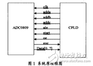
Among them: ALE: is the address latch enable input line, active high. When ALE is high, the address latches and the address signals of the three address lines of the decoders ADDA, ADDB, and ADDC are latched, and the selected channel analog quantity is converted into a converter after being decoded. ADDA, ADDB, and ADDB are address input lines that are used to strobe an analog input on IN0-IN7.
START: Starts the A/D conversion control pin, and the falling edge of the level is valid. Data[0..7]: AD conversion data output.
OE: Data output enable control terminal, when the high level is valid, the data output tristate gate is opened, and the converted data amount is sent to the Data[0..7] pin; when invalid, Data[0. .7] The feet are suspended.
CLK: ADC working clock input pin, clock frequency range 10KHz~1280KHz, the system is set to 500KHz.
EOC: ADC conversion end status signal, low level indicates that conversion is in progress, duration is A/D end time, and low level transitions to high level to indicate end of conversion. This signal is for the CPLD to query.
System module design ADC0809 sampling control moduleThe ADC0809 sampling control adopts the molar state machine control for analog-to-digital conversion. According to the working timing diagram of AD shown in Figure 2, the sampling control process is divided into seven states:
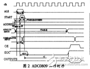
Initialization state: ADC0809 sampling control signal is initialized, and each sampling control status signal is set to zero.
Address Latch Status: With the rising edge of ALE, the address of the 8-channel sampling input channel of ADC0809 is entered into the ADC0809 address locker.
Start 8-bit converter: Turn on the ADC0809 start signal START.
Wait for conversion: Detects the end of conversion signal EOC signal.
Output valid state: 8-bit parallel data output is allowed.
Output latch data: Turn on the data latch signal LOCK. This allows another process to detect the latch signal LOCK, which latches and stores the converted data on its rising edge.
Return to initial state
Clock generation moduleThis system uses a 20MHz crystal oscillator, because ADC0809's operating frequency is 500KHz, in addition, a 40KHz scan address signal is required when switching channels. Therefore, it is necessary to divide the 20 MHz signal to generate 500 KHz and 40 KHz signals.
Sampling channel controlIn the AD sampling control module, a process is used to detect a clock signal having a clock frequency of 40 kHz, and one sampling must be completed within the clock cycle . When the rising edge of the signal arrives, the sampling channel is switched, and the eight channels are sequentially patrolled.
CPLD software designThe CPLD program is written in VHDL under the QUARTUS8.0 software environment. There are mainly frequency division modules and the ADC0809 module controlled by the mole state machine. The simulation uses the simulation tool that comes with QUARTUS8.0. The simulation results are shown in Figures 3 and 4:
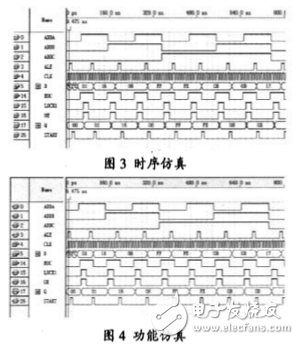
It can be seen from the simulation results that it meets our design requirements.
Mini Jumper Connector,2.54Mm Mini Connector,Mini 2.54Mm Connector,2.54Mm Mini Jumper Connector
Dongguan Yangyue Metal Technology Co., Ltd , https://www.yyconnector.com