Abstract—A high-performance GaAsSb base for RF and microwave test systems. The InP collector DHBT IC process was successfully developed. This GaAsSb process allows fT and fmax to reach 185 GHz and 220 GHz at an operating current of JC = 1.5 mA/μm2 and an open-state breakdown voltage of BVcbx = 9 V at JC = 1.3 mA/μm2. Typical ï¢ = 50. Maximum operating conditions (Tj = 125 oC, JC = 2.0 mA/μm2) reach MTTF 1 &TImes; 106 hours of life make it suitable for test level applications. DHBTs integrate 3 layers of interconnect metal, including 2 levels of resistors and MIM capacitors. This IC technology has been used to manufacture Agilent Technologies instrumentaTIon products on the 3†production line.
I. IntroductionA high-performance GaAsSb base region for RF and microwave test equipment, the InP collector region double heterojunction bipolar transistor integrated circuit (DHBT IC) process was successfully developed. Its unique high RF power and unit area gain, excellent gain and turn-on voltage uniformity, large transconductance, low 1/f and phase noise make HBT IC an advanced technology that is very attractive for test instruments.
InP technology extends the original InGaP/GaAs heterojunction bipolar transistor integrated circuit HBT IC technology [1][2], enabling test instrument performance to reach 67 GHz and 54 Gb/s without sacrificing reliability and manufacturability. . InP has superior material properties compared to GaAs, such as higher saturation and peak electron velocity, higher thermal conductivity, lower surface recombination rate, and higher breakdown electric field strength. However, in the conventional GaInAs base region/InP collector region double heterojunction bipolar transistor DHBT, there is a collector junction heterogeneous interface conduction band discontinuity. Solving the problems caused by this type I semiconductor band structure requires careful design of the band gradient to eliminate electron blockage in the collector region at low bias. In contrast, GaAsSb is selected as the base region, and InP can be used as a collector region to form a non-blocking effect.
Type II semiconductor band structure while maintaining a low turn-on voltage and low power consumption of a narrow baseband bandgap [3]. Combined with its good thermal characteristics in complex circuits, the high-speed, high-breakdown heterojunction bipolar transistor HBT with GaAsSb/InP as the base/collector is ideal for test instrumentation.
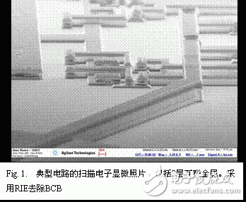
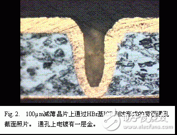
II. Preparation processThe fabrication process uses 1 μm critical dimension G-line step lithography. The epitaxial layers of the heterojunction bipolar transistor HBTs are grown by a molecular beam epitaxy method on a semi-insulating InP substrate to form a 1 &TImes; 3 μm 2 minimum size emitter and a self-aligned evaporation base metal electrode. Preparation of emitter mesas by selective and non-selective wet etching processes, and non-selective Cl2/Ar-based inductively coupled plasma (ICP) dry etching processes, base ohmic contact electrodes, base/collection Area countertop, sub-collector area isolated countertop. Plasma enhanced chemical vapor deposition (PECVD) Si3N4 is used as a passivation medium. The transistor integrates a 22 ohm/sq Ta2N resistor, a 250 ohm/sq WSiN resistor and a PECVD deposited Si3N4 0.58 fF/μm2 metal-dielectric-metal MIM capacitor. Polyphenylenecyclobutene (BCB) is used to planarize the surface of the device, and the emitter, base, collector ohmic contact electrode, and other passive cells are metal interconnected by electrode metal deposition. The metal interconnect uses three layers of TIPtAu: the first two layers are 6 μm electrode contact holes and the third layer is 8 μm electrode contact holes (Fig. 1). The substrate was thinned to 90 μm. Back grounding is achieved by etching the back via and gold plating (Fig. 2). The back via is achieved by a mask and HBr-based ICP etching [4].
Literature [5] [12] introduced some other InP double heterojunction bipolar transistor integrated circuit DHBT IC technology, which use GaInAs as the base region. The GaAsSb-based double heterojunction bipolar transistor DHBT has been continuously reported in high-speed RF discrete devices [13] [14] and integrated circuits [15] [16]. This work is the first to report the DHBT IC process of InP double heterojunction bipolar transistor integrated circuit with high breakdown voltage, 200 GHz operation and GaAsSb as the base region.
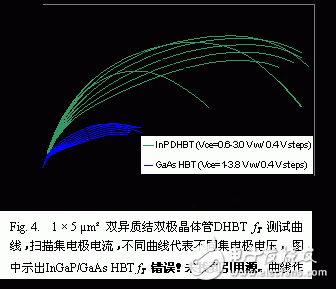
Typical HBT common emitter DC characteristics (collector current—collector bias, base current interval 30 μA) show good current-voltage characteristics of these devices (Fig. 3). At an operating current density of 1.5 mA/μm2, the HBT device achieves fT = 185 GHz, fmax = 220 GHz and peak fT "200 GHz. The cutoff frequency is kept at a very high level in the current density range much larger than the InGaP/GaAs HBT (Fig. 4).
The common base mode on-state breakdown voltage (BVcbx) occurs when the collector-base voltage is 9 V and the collector current is JC = 1.3 mA/μm2. Common emitter mode on-state breakdown (BVceo) occurs when the collector-emitter voltage is close to 7V.
IV. Productivity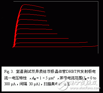
Insulation Tubes,Pvc Pipe Insulation,Insulated Pex Pipe,Rubber Insulation Tube
Shenzhen Huiyunhai Tech.Co., Ltd. , https://www.cablesleevefactory.com