The main points of the audio guide are as follows: One is to receive the navigation information of the working satellite through the user terminal of the Global Positioning System (GPS), thereby calculating the latitude and longitude information of the vehicle, and then calculating the real-time coordinates, and the coordinates of the attraction. In comparison, when the vehicle enters a certain distance of the scenic spot, the system automatically broadcasts the scenic phone voice information without manual intervention; the other is to count the corner pulse of the wheel axle, and compare the count value with the preset value to determine At the moment of playing, the purpose of accurately playing the voice information of the scenic spot is achieved; the third scheme is to use radio frequency identification technology to set a radio frequency transmitter with a unique ID in each scenic spot, and use intermittent operation to transmit signals when the tourist train is about to When arriving at the attraction, the in-vehicle system receives the RF transmitter signal and decodes the ID number of the attraction, and the system controls to automatically play the corresponding number of scenic voice information. Due to the complexity of the natural environment of the scenic spot, the first method is difficult to meet the system requirements; the second method is simple and reliable, but the traveling direction of the tourist rail vehicle is uncertain, its relative position changes back and forth, and the degree of automation of the system is low and complicated. Higher. This paper adopts the third scheme to realize the automatic navigation system of scenic spots.
This paper first introduces the overall structure of the system, then gives the specific design of the main functional modules of the system, and focuses on the SPI communication control and implementation technology between the STM32F103RBT6 chip based on ARM3 core and the voice chip ISD4004, and gives the system. Design the implementation results.
Finally, the conclusions of the reference value of certain engineering applications are given.
1 overall system design
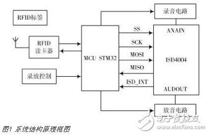
The structural principle design of this system is shown in Figure 1. The design utilizes the characteristics of the fixed train track, pre-installed fixed ID RFID in the scenic spots along the track, taking into account the working distance, data communication mode, reliability, service life and maintenance cost, and selects the product 433 MHz active tag GAO C124061. Its storage ID word length is 32 b. Because in the natural environment of the wild, the possibility of collision is extremely low, the RFID reader only needs to correctly and reliably obtain the ID value of the RFID, corresponding to the fixed attraction, to trigger the interruption and start playing the voice information of the attraction.
In Figure 1, the MCU uses the STM32F103RBT6 chip, which is a high-performance, low-cost, low-power embedded application MCU based on the ARM Cortex-M3 core. The reason for this design choice is to pay attention to its cost performance: 128 KB FLASH, 20 KBSRAM, 2 SPI, 3 serial ports, 1 USB, 1 CAN, 2 12-bit ADC, RTC, 51 available I/O A series of performance characteristics such as feet can fully meet the performance requirements of this system. To sum up, STM32 has several advantageous advantages such as low price, strong function, simple use and convenient development. The ISD4004 is a voice recording and playback memory chip that can be randomly recorded for voice recording and voice playback according to external control and peripheral circuit assistance. The system MCU obtains the fixed ID of the RFID along the travel train through the RFID reader. According to the start address information of the preset voice data storage location corresponding to the ID number, the SPI port built in the ISD4004 is controlled to realize the automatic playback of the scenic voice segment.
2 main module circuit design
2.1 ISD4004 control circuit design
The ISD4004 series voice chip has a working voltage of +3 V, and the recording and playback time of the single chip is 8~16 min, and the sound quality is good. The chip uses CMOS technology and includes a clock, anti-aliasing filter, smoothing filter, audio amplifier, auto-squelch and high-density multi-level non-volatile memory array. The chip design is based on all operations must be controlled by the microcontroller, and operational commands can be sent via the serial communication interface (SPI). The chip uses multi-level direct analog storage technology, each sample value is directly stored in the on-chip non-volatile memory, so it can reproduce the voice, music, tone and effect sound very realistically and naturally, avoiding the general solid-state recording circuit. Quantization noise and metal sound due to quantization and compression. The internal structure and main pin functions of the chip ISD4004 are shown in Figure 2.
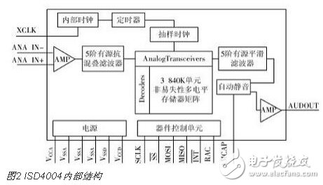
The ISD4004 internal device control unit is very easy to set up for communication with the SPI of the STM32 serial chip. Multiple STM32 I/O ports can be added to serve as the chip select terminal for the corresponding voice chip, so that multiple ISD4004 extensions can be realized. The interface circuit between STM32 and multi-chip ISD4004 is shown in Figure 3.
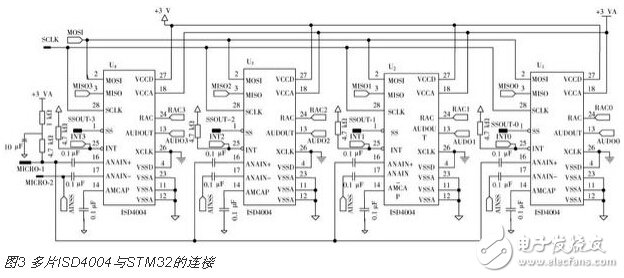
The STM32 and ISD4004 communicate through the SPI module. The MOSI and MISO pins are connected to each other to realize serial data transmission between the STM32 and the ISD4004 (the MSB bit is first). Communication is always initiated by the master STM32. The STM32 sends the data to the ISD4004 via the MOSI pin, and the ISD4004 passes back the data to the STM32 via the MISO pin.
The data output and data input of full-duplex communication are synchronized by the same clock signal; the clock signal is provided by the master STM32 via the SCK pin.
After being expanded into multiple voice chips, the storage space of voice information is greatly increased, which is convenient for expanding the voice information of the attraction.
2.2 Voice Recording Control Circuit Design
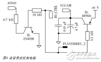
The voice recording and playback control circuit is shown in Figure 4. The series adjustment tube Q3 or the switch tube Q1 is controlled by the I/O control terminal of the MCU to realize system playback or recording. The recording is realized when the I/O terminal outputs a high level, and the playback is performed when the output is low.
2.3 RFID card reader interface circuit
The RFID reader module uses Philips' highly integrated ISO14443A reader chip MFRC500. The RFID reader is a relatively independent function module whose output can be connected to the outside through interrupt status information and serial port. Therefore, the system uses the SPI2 interface of the STM32F103RBT6 to implement data communication with the RFID reader interface, thereby automatically obtaining the location information of the attraction to control the selection of the corresponding scenic navigation voice. The reader interrupt status is directly connected to the PD port I/O pin of the STM32F103; the SPI2 interface circuit is similar to Figure 3.
3 main function software design
3.1 Software initialization
3.1.1 Peripheral Clock Enable
The peripheral clocks involved in this design can be enabled through the APB2 peripheral clock enable register. When the peripheral clock is not enabled, the software cannot read the value of the peripheral register, and the returned value is always 0. The clocks of the PA port, PB port, and PD port used in the design pass the 2nd and 3rd of the APB2ENR register respectively. Set by 5 bits, the clock of SPI1 is set by the 12th bit of APB2ENR.
3.1.2 Initialization of I/O Port
The I/O ports involved in this design include: PA.3 and PB.0 ports for controlling chip select expansion, which need to be set to the open end output mode; PA.15 (recording key) for implementing button control, PA.0 (Forced stop button), etc. should be set to pull-up input mode; PA.5, PA.6, PA.7 ports for SPI communication, which correspond to SCK, MISO, MOSI ports of SPI1, respectively, should be set by software The three ports are the second function of the multiplexed I/O port; the PA.8 and PD.2 for detecting the low level output of the INT terminal of the voice chip at the end of the playback are set to the pull-up input mode.
3.1.3 Initialization of External Interrupts
The main work done in the external interrupt initialization is to set the correspondence between the I/O port and the interrupt line, turn on the online interrupt/event corresponding to the I/O port, set the trigger condition of the interrupt, configure the interrupt packet, and enable the interrupt. . In this design, the interrupt trigger condition corresponding to the PA.0 port to which the forced stop button is connected is set to the rising edge trigger, and the corresponding interrupt priority is the highest; the interrupt trigger conditions corresponding to the remaining I/O ports of the button are set to decrease. Trigger along the edge. All interrupts are assigned to the second group, the secondary priorities of all buttons are set to the same, and the preemption priorities are different. Among them, the interrupt corresponding to the I/O port connected by several playback keys shares an interrupt service program, that is, the interrupts on multiple interrupt lines share an interrupt service function, and the interrupted service program first enters the interrupted signal. Make a distinction (by judging the level on the input I/O port) and then process it separately.
3.1.4 Initialization of the SPI module
In this design, the SPI1 module is set to full-duplex mode, software NSS management, host mode, 8 b MSB data format by setting the CR1 register, and the baud rate of SPI1 is set to the lowest (281.25 kHz for the system). The clock is divided by 256. The most important one is the configuration of the SPI module output serial synchronous clock polarity and phase. The phase and polarity of the SPI master module and the external device communicating with it should be the same. Finally, send 0xff to start the transfer.
According to the SPI bus transmission timing and SPI operation timing relationship in different phases of ISD4004, in order to realize SPI communication between STM32 and ISD4004, its control bits CPHA and CPOL must be set to 1.
3.2 SPI control function software implementation
3.2.1 SPI1 read and write byte function
When reading data, the received data is stored in an internal receive buffer; when writing data, the data is first stored in an internal transmit buffer before being sent. A read to the SPI_DR register will return the contents of the receive buffer; the data written to the SPI_DR register will be written to the transmit buffer.
SPI_SR is a 16-bit status register. Its lowest bit is RXNE. If the bit is 0, the receive buffer is empty. If it is 1, the receive buffer is non-empty. The lower-order bit of SPI_SR is TXE. If the bit is 0, the transmit buffer is not empty. 1 The send buffer is empty. Continuously query whether the send/receive buffer is empty, thereby achieving orderly transmission and reception of data.
3.2.2 Send instruction function
First, the voice chip ISD4004 has the following operational rules:
(1) Serial peripheral interface, SPI protocol setting The SPI shift register of the microcontroller operates on the falling edge of SCLK, latching the MOSI pin data on the rising edge of the clock, and sending the data to the MISO pin on the falling edge.
(2) The power-up sequence, the device delay TPUD (about 25 ms at 8 kHz sampling) can not start operation. Therefore, after the user completes the power-on command, the user must wait for the TPUD to issue the next operation command.
For example, to play from 00, the following sequence should be followed:
1 send a POWER UP command;
2 Wait for TPUD (power-on delay);
3 Send a SET PLAY command with an address value of 00;
4 Send the PLAY command.
The device will start playing from the 00 address. When the EOM appears, it will be interrupted immediately and the playback will stop.
If you are recording from 00, the following sequence is used:
1 issued a POWER UP command;
2 Wait for TPUD (power-on delay);
3 send a POWER UP command;
4 waiting 2 times TPUD;
5 Send a SET REC command with an address value of 00;
6 Send a REC command.
The device starts recording from the 00 address and stops recording until OVF (end of memory) appears.
3.3 Interrupt Service Procedure
The recording interrupt service program flow is shown in Figure 5. The function realized by it is to record the voice information of an attraction into the ISD4004 in a preset starting address storage space when the recording button is pressed for a long time. After the recording button is released, the recording of the voice content of the attraction stops. The location of the navigation of each attraction's navigation is indicated by its starting address. The arrangement of the starting address is determined by the length of each speech. When recording the voice of each attraction, keep the recording button locked and not release until the end of the audio recording of this section.
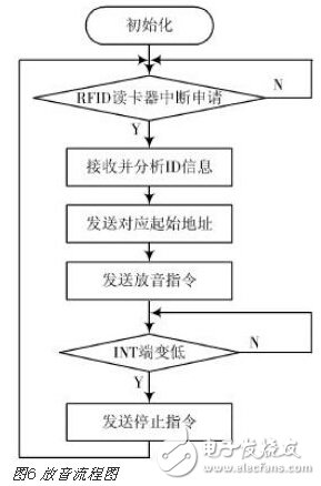
The program flow interrupt service program flow is shown in Figure 6. After obtaining the interrupt request of the RFID card reader, according to the card reader interface protocol, the MCU receives the data information transmitted by the card reader via the SPI2 interface, and analyzes the ID information content of the RFID, and according to the ID corresponding to The location of the attraction, that is, the original address of the original location voice, sends the first address to the ISD4004 chipset, and sends a playback command, which can realize the automatic playback of the navigation voice recorded in advance by the corresponding attraction. While the voice message is starting to play, the INT- terminal of the ISD4004 is connected to the I/O port of the STM32, constantly queried for its status. When the voice information is finished, the INT-end of the voice chip ISD4004 is de-asserted, thereby transmitting a stop-play command, and the broadcast ends, and waits for the next RFID message input and the card reader interrupt request.
![]()
4 system debugging test results
4.1 Recording and playback module debugging
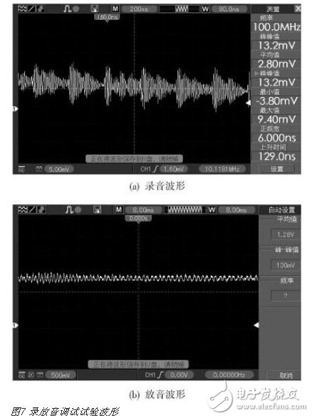
For the test of the function of the recording module, the following method is adopted: playing the sound against the microphone, and using an oscilloscope to observe whether the input pin of the voice chip has a signal. A signal is detected at the voice chip input pin as shown in Figure 7(a).
After the voice is successfully entered, the playback command is sent to the voice chip output pin to obtain the waveform shown in Figure 7(b).
4.2 SPI module debugging
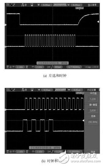
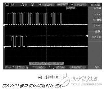
After the recording circuit is correct, send a playback command. On the pin end of the chip corresponding to the SPI1 module function, you can see the correct timing on the oscilloscope, as shown in Figure 8.
Figure 8(a) shows the chip select and clock signal output; Figure 8(b) and (c) are the waveforms obtained by continuously transmitting O&Tmes; 55, the data transmitting end MOSI and the data receiving end MISO of the STM32 SPI1, respectively. Actually match.
5 Conclusion
The system proposed in this paper is simple, practical and reliable, and is especially suitable for the orbital tourist train projects in mountainous natural attractions. Therefore, the system has good practical value. It can be used to implement the structure of the audio navigation system in complex environment. The implementation technology and debugging experiment results of the main functional modules of the system are introduced in detail.
Carbon Fiber Rigid Felt Tube,Vacuum Furnace Insulation Cylinder,Carbon Fiber Thermal Insulation Cylinder,Heat Insulation Screen Of Vacuum Furnace
HuNan MTR New Material Technology Co.,Ltd , https://www.hnmtr.com