Circuit function and advantage
S/PDIF (Sony/Philips Digital Interface) is a high quality digital audio format commonly used in consumer electronics devices for the interconnection of audio devices. Many audio codecs/DSPs only support I2S as a digital audio input/output, which can cause problems when used in circuits that require both S/PDIF and AES (Audio Engineering Association) professional standards.
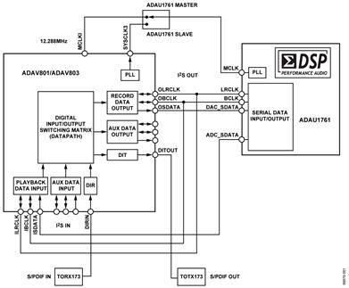
   The circuit shown in Figure 1 connects the audio codec ADAV801 or ADAV803 to a SigmaDSP device such as the ADAU1761 to solve this problem.
The audio input of the S/PDIF format is first converted to the I2S format and then processed by the ADAU1761. The processed I2S format audio output is converted back to the S/PDIF format by the ADAV801/ADAV803. The ADAV801/ADAV803 features a flexible digital input/output routing matrix that can handle audio in I2S or S/PDIF format and can be output in any format; with on-chip SRC (Sampling Rate Converter), it can be used as a master Or slave device. The ADAV801/ADAV803 supports the consumer audio standard, and channel status data can be embedded in the audio stream by writing to the relevant registers in the ADAV801/ADAV803. This feature can be used to transfer configuration information between devices. The ADAV801/ADAV803 has a stereo DAC/ADC that can be used to process audio when needed.

Figure 1. Connecting S/PDIF Input/Output with the ADAU1761 via the ADAV801/ADAV803
Circuit description
The ADAV801/ADAV803 has two sets of input/output I2S ports, which can be used in any group. In the configuration shown in Figure 1, the playback port ILRCLK pin and the recording port OLRCLK pin are connected to the LRCLK pin of the ADAU1761. The IBCLK and OBCLK pins are connected to the BCLK pin of the ADAU1761. The ISDATA pin is connected to the ADC_SDATA pin of the ADAU1761, and the OSDATA pin is connected to the DAC_SDATA pin of the ADAU1761.
The S/PDIF input comes from the TORX173 fiber optic receiver module, enters the DIRIN pin, and then outputs to the ADAU1761 through the recording port in I2S format. The audio is processed by the ADAU1761 SigmaDSP? device and output to the ADAV801/ADAV803 through the ADC_SDATA pin in the I2S format. The playback port is then converted to S/PDIF format and sent to the TOTX173 fiber optic transmitter module via the DITOUT pin.
The circuit is powered from a 3.3 V AVDD supply. The main clock of the circuit is generated by the ADAV801/ADAV803 or an external oscillator, depending on whether the ADAU1761 is configured as a master or a slave. When the ADAU1761 is used as a slave, ie, BLCK and LRCLK are driven by the ADAV801/ADAV803, MCLK is 256 times the audio clock recovered from the S/PDIF stream. It can also be configured to be equal to 512 times the recovery clock. This clock is accessed through the SYSCLK3 pin of the ADAV801/ADAV803 and is connected to the MCLK pin of the ADAU1761.
When the ADAU1761 is the master device, MCLK is generated by the on-chip oscillator and supplied to the ADAV801/ADAV803 through the MCLKI pin. In this case, the ADAU1761 drives the LRCLK and BCLK lines, and the SRC on the ADAV801/ADAV803 is used to synchronize the I2S port and S/. Audio between PDIF ports.
Register setting
For a complete design support documentation package for this circuit note, see , which includes register settings for the ADAV801/ADAV803 and ADAU1761 in both master and slave configurations. These register settings files can be loaded using the associated EV kit software.
Common changes
This circuit can also be configured with any device that has a SigmaDSP processor core and requires an S/PDIF/AES audio interface, including the ADAU1401A, ADAU1701, and ADAU1781. Although not noted in this circuit note, the above circuit can be modified to handle AES audio. format. An XLR connector can be used instead of a fiber optic connector, in which case a transformer is needed to convert the differential signal to a single-ended signal and vice versa.
Circuit evaluation and testing
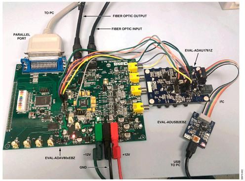
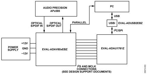
This circuit is tested using the ADAV801/ADAV803 evaluation board (EVAL-ADAV801EBZ or EVAL-ADAV803EBZ) and the ADAU1761 (EVAL-ADAU1761Z) evaluation board. See the design support documentation for the required connections and link configurations between the evaluation boards. Figure 2 shows the complete test setup using two evaluation boards.
Equipment requirements
The ADAU1761 evaluation board is programmed with SigmaStudio via a USBI board (EVAL-ADUSB2EBZ). The SigmaStudio GUI software requirements for PC are as follows: Windows 7, Windows Vista, Windows XP Professional or Home Edition (SP2); 128 MB RAM (256 MB recommended); 50 MB free hard disk space; 1024 × 768 screen resolution; USB 1.1/ 2.0 data port. The ADAV801/ADAV803 board is controlled using the PC's printer port, and the associated control software can be downloaded from the Analog Devices website. Connect the S/PDIF input/output to the ADAV801/AD
The AV803 evaluation board requires 2 fiber connectors. To make the necessary connections between the two evaluation boards, eight single-pin jumper cables are required.
start using
Then, refer to the documentation for the EVAL-ADAU1761Z and EVAL-ADAV801/ EVAL-ADAV803EBZ for software installation, setup, and system operation.
Use SigmaStudio software to set and adjust the registers of the ADAU1761 and the SigmaDSP core. To download SigmaStudio, please visit:
Software for the ADAV801/ADAV803 can also be downloaded from the ADI website. Once the software installation is complete, the EV kit can be programmed by loading the appropriate register settings file in the design documentation, depending on whether the ADAU1761 is used as a master or a slave. The ADAU1761 SigmaStudio project has only a simple audio transfer function with volume control to test the circuit shown in Figure 1.

Figure 2. Test setup for connecting the ADAV801/ADAV803 evaluation board to the ADAU1761 evaluation board

Figure 3. Test setup functional block diagram
Setup and testing
The Audio Precision APx585 multichannel audio analyzer can be used to generate S/PDIF inputs and capture S/PDIF outputs. When the ADAU1761 is used as a master, the total harmonic distortion plus noise (THD + N) at the S/PDIF output should be approximately 130 dB for a full-scale 1 kHz input tone. In slave mode, THD + N should be Approximately 142 dB because no SRC is needed to synchronize the S/PDIF stream with the ADAU1761 I2S stream.
CIRCUITS FROM THE LAB Lab Circuit
Built and tested to ensure functional and performance circuit design.
A variety of common analog, RF/IF, and mixed-signal design challenges are addressed with ADI's extensive application expertise.
Equipped with complete documentation for easy learning, understanding and integration.
The diameter of the DO-41 diode body is in the range of 2.0mm~2.7mm, the length of the diode body is between 4~5.2mm, the diameter of the pins at both ends is between 0.71mm~0.86mm, and the overall length is 25.4mm.
This DO-41 plastic package is available in a through-hole version. This axial lead device is ideal for customer premises equipment (CPE), such as telephones, answering machines, modems, and fax interfaces. When appropriate over-current protection is included, the DO-41 package series can also be used for over-voltage protection in applications such as T1/E1/J1 relay cards.
DO-41 package,Rectifier Diode,General Porpose Rectifiers Diode,General Porpose Rectifiers
Changzhou Changyuan Electronic Co., Ltd. , https://www.changyuanelectronic.com