0 Introduction <br> With the rapid development and widespread adoption of wireless communications, wireless system standards are increasingly demanding transceiver performance. As the main component of the transmitter, the power amplifier determines the performance of the transmitter. For example, the efficiency determines the power consumption of the whole machine. The linearity determines the dynamic range of the whole machine. The harmonic component is the measure of the linearity of the transmitter. . Conventional Power Amplifiers In order to achieve higher efficiency, the power amplifier tube usually operates in a saturated state, where a large amount of harmonic components are generated. If the harmonic components are not recovered and suppressed, this will not only cause waste of energy, reduce its efficiency, but also cause interference to signals of other channels.
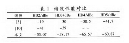
Generally, the power amplifier operates the power amplifier in the F class in order to obtain higher efficiency and lower harmonic components, but the structure needs to adopt a λ/4 transmission line, which has a large space and is not conducive to miniaturization. A low-pass output matching network is used to design a power amplifier operating in class E. The 2nd to 5th harmonic components at 11 dBm input are: -19 dBc, -30 dBc, -38.5 dBc, and -41.7 dBc. However, this structure uses a class E amplifier, which requires a higher collector breakdown voltage of the power amplifier tube, which is contrary to the development trend of the integrated circuit. In order to obtain better harmonic performance, the power amplifier designed by GaN process introduces two open transmission lines in the output matching network, but the use of open transmission lines makes the method and modern circuit to be smaller and more integrated. Development is contrary.
In this paper, an output matching network with simple structure, integration and harmonic suppression is proposed. A power amplifier operating at 2 GHz is designed by InGaP/GaAs HBT process. The test results show that the power amplifier designed by this method achieves high efficiency and good harmonic performance.
1 Circuit Design <br> A typical power amplifier usually consists of an input matching network, an amplifying circuit, a DC bias circuit, and an output matching network. However, it is the matching network that plays a decisive role in the performance of the power amplifier. As an important part of the power amplifier, any unsuitable matching network may cause instability of the circuit, resulting in low power output, low efficiency, and deterioration of linearity. When designing a matching network, while satisfying the basic impedance transformation, it must also take into account its harmonic impedance, insertion loss and bandwidth of the network. Finally, it is necessary to consider whether the designed network is easy to implement and miniaturized.
1.1 Output matching network with harmonic suppression The output matching network is the most important part of the matching network, which determines the power and efficiency of the power amplifier and the harmonic performance of the final power amplifier. The literature [6-7] specifies the effect of the second harmonic impedance of the output matching network on its efficiency, but ignores the influence of higher harmonics. The output matching network designed in this paper considers the second harmonic impedance while taking into account the higher harmonic impedance. Its structure is shown in Figure 1.
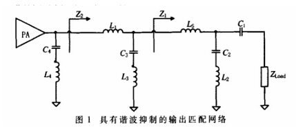
Among them, C1 acts as a blocking function, and L1, C3 and L5, C2 form a two-level low-pass network. At the fundamental frequency, it mainly acts as an impedance transform, exhibiting high impedance at high-order odd harmonics, and C4 and L4 form a In series LC resonant network, the resonant frequency is 2ω0, where ω0 is the fundamental frequency, so that the output network gets a short-circuit load at the second harmonic. This structure is similar to the Class F power amplifier [8]. It exhibits high impedance for odd harmonic loads and low impedance for even harmonic loads, which is beneficial for shaping the output voltage and current waveform of the power amplifier tube. The overlap makes the efficiency [9]. At the same time, in order to recover and suppress the higher harmonic energy, two inductors L3 and L2 are added to the two-stage LC low-pass matching, which form a series resonant network with C3 and C2, and the resonant frequencies are 3ω0 and 5ω0, respectively. That is, the 3rd harmonic and the 5th harmonic are processed separately. The analysis of the output matching structure is as follows: For the load of the power amplifier tube, the relationship between its value and output power is:

In order to obtain better network bandwidth, the impedance of the intermediate level of the two-stage LC low-pass matching network is:

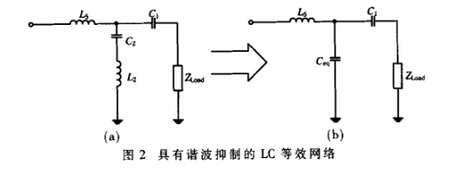
For a harmonic processing network composed of LC, when the resonance is at a higher harmonic frequency, at the fundamental frequency, the network is equivalent to a capacitor, as shown in Figure 2, setting the L2C2 resonance at the nth harmonic (Fig. 2(a)), at the fundamental frequency it is equivalent to the capacitance Ceq1 (Fig. 2(b)), the relationship is:

When operating at the fundamental frequency, the impedance of the network is:

The two types of simultaneous (3) (4) are:

That is, the relationship between the equivalent capacitance of the resonant network at the fundamental frequency and the capacitance of the resonant network is:

For this design, because the L2C2 resonance is at the 5th harmonic frequency, the L3C3 resonance is at the 3rd harmonic frequency, so there are:
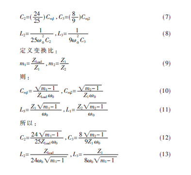
For the series resonant network composed of L4C4, the resonant frequency is 2ω0, which is mainly used to recover the 2nd harmonic energy, which can shape the voltage and current waveform at the output end of the power amplifier tube, reduce the coincidence between the two, and improve the power amplifier. s efficiency. The following relationship is satisfied between the capacitor and the inductor:

1.2 Overall Circuit Design Using the InGaP/GaAs HBT process, an InGaP/GaAs HBT process is used to design a power amplifier with high efficiency and high harmonic rejection at 2 GHz. The amplifier uses three-stage amplification. Structure, the supply voltage is 5 V, the specific circuit structure is shown in Figure 3.
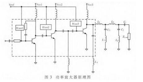
The design uses a three-stage amplification structure in order to obtain high gain, in which the first stage operates in the class A state to obtain high linearity, the stage uses an RC negative feedback to make the circuit work stably; the second stage works in Shallow AB class state; third class works in deep AB class state in order to achieve high efficiency. The part in the dotted line box is realized on-chip, and the part outside the box is realized by using a multi-layer substrate, a binding line and a patch element. For the inter-stage matching network, the matching inductor is implemented on the external binding line to help reduce the insertion loss of the inter-stage matching network, and obtain higher efficiency and power, and the debugging is flexible and convenient. For the output matching network, where L4 is composed of the bonding line and the transmission line on the substrate, the size of the second harmonic component can be controlled by adjusting the length of the gold wire. For L3 and L2, since the network suppresses higher harmonics, the required inductance is small, which is mainly composed of via holes of the multilayer substrate.
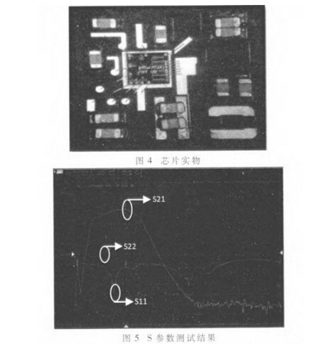
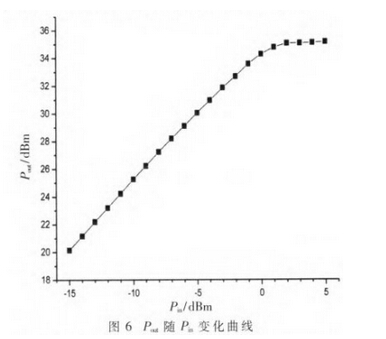
2 Test Results <br> This chip is fabricated by InGaP/GaAs HBT process. Figure 4 shows the physical picture of the chip. The DIE area is 1 mm × 1 mm, and the overall package size is 4 mm × 4 mm. Figure 5 shows the S-parameter test results of the design. The test platform is the Agilent Vector Network Analyzer E5071C. The test results show that the S-parameters of the design at 2 GHz are: S21=35.1 dB, S11<-10 dB, S22<-10 dB. From the S-parameters, the design achieves good small-signal performance. Figure 6 is the relationship between output power and input power. It can be seen from the figure that when Pin is less than 0 dBm, the amplifier works in linear operation. When Pin is greater than 0, compression begins to appear. When it reaches 3 dBm, the output power is saturated. Pout = 35.2 dBm and the amplifier's 1 dB compression point is P1dB = 34.2 dBm.
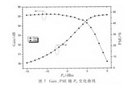
As can be seen from the figure, the amplifier achieves better linearity. Figure 7 is a graph of gain Gain and efficiency PAE as a function of input power. The graph shows that the gain of the design is less than 0.2 dB at Pin<0 dBm, indicating that the design achieves good AM-AM. When operating at saturation, ie Pout = 35.2 dBm, the efficiency is PAE = 48%; when operating at 1 dB compression point, ie Pout = 34.2 dBm, the efficiency is PAE = 43%. As can be seen from the efficiency graph, the amplifier not only achieves high efficiency in saturation operation, but also achieves good efficiency in linear operation. Table 1 compares the harmonic performance of this design with other designs. It can be seen from Table 1 that this design considers the second harmonic and also takes into account the higher harmonics, achieving good harmonic suppression, especially in the high order. Harmonic processing.
3 Summary <br> This paper introduces multiple LC resonant networks in the output matching network of the power amplifier to recover and utilize the harmonic energy of the power amplifier, which improves the efficiency of the power amplifier and suppresses the harmonic components of the load. The method is simple, easy to implement and facilitates miniaturization of the power amplifier. Using this method, a power amplifier operating at 2 GHz is designed. The measured results of the power amplifier are: Gain=35 dB, 1 dB compression point is P1dB=34.2 dBm, and saturation efficiency is PAE=48%. The harmonic component sizes are: HD2=-53 dBc, HD3=-58 dBc, HD4=-65 dBc, HD5=-60 dBc. The test results show that the power amplifier designed by this method achieves good efficiency and harmonic performance.
Full Outdoor Digital Signage,Full Outdoor Signage,Waterproof Lcd Display,High Brightness Digital Signage
Shenzhen Risingstar Outdoor High Light LCD Co., Ltd , https://www.risingstarlcd.com